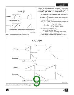
AN-32
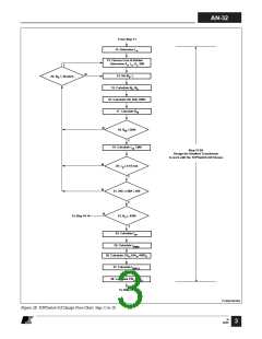
From Step 28
29. Select Clamp Zener & Blocking Diode
30. Select Output Rectifier
31. Select Output Capacitor
32. Select Output Post Filter L, C
33. Select Bias Rectifier
34. Select Bias Capacitor
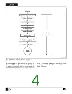
Step 29-37
Select Other Components
35. Select CONTROL Pin Capacitor
& Series Resistor
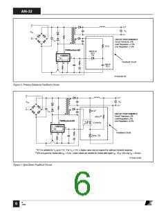
36. Select Feedback Circuit Compenents
According to Reference Feedback Circuits
in Figures 3, 4, 5 and 6
37. Select Bridge Rectifier
Design
Complete
PI-2584-091402
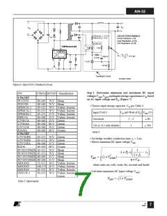
Figure 2C. TOPSwitch-GX Design Flow Chart. Step 29 to 37.
The overriding objective of this procedure is “design for cost
effectiveness.” Using smaller components usually leads to a
less expensive power supply. However, for applications with
stringent size or weight limitations, the designer may need to
strike a compromise between cost and specific design
requirementsinordertoachievetheoptimumcosteffectiveness
for the end product.
B
12/02
4

 ETC [ ETC ]