AN-32
• Gap length in mm: Lg ≥ 0.1
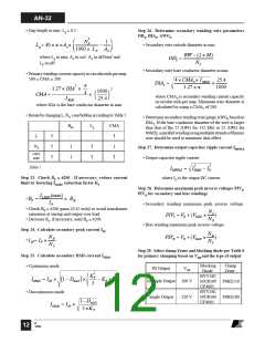
Step 26. Determine secondary winding wire parameters
ODS, DIAS, AWGS
NP2
1
• Secondary wire outside diameter in mm
Lg= 40 × π ×Ae ×
−
1000 × L
A
L
P
BW − (2 × M)
where Lg in mm, Ae in cm2, AL in nH/turn2 and
ODS =
NS
LP in µH
• Secondary wire bare conductor diameter in mm
• Primary winding current capacity in circular mils per amp:
500 ≥ CMA ≥ 200
4 × CMAS × ISRMS 25.4
DIAS =
×
1.27 × DIA2 ×
π
1.27 × π
1000
2
1000
25.4
4
CMA =
×
where CMAS is secondary winding current capacity
in circular mils per amp. Minimum wire diameter is
calculated by using a CMAS of 200.
IRMS
where DIA is the bare conductor diameter in mm
• Iterate by changing L, NS, core/bobbin according to Table 7.
• Determine secondary winding wire gauge AWGS based on
DIAS. If the bare conductor diameter of the wire is larger
than that of the 27 AWG for 132 kHz or 25 AWG for
66kHz,aparallelwindingusingmultiplestrandsofthinner
wire should be used to minimize skin effect.
BM
-
Lg
-
CMA
L
↑
↑
↑
↑
↑
↑
NS
↑
↑
Step 27. Determine output capacitor ripple current IRIPPLE
core
size
↑
↑
• Output capacitor ripple current
IRIPPLE = IS2RMS − IO2
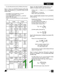
Table 7.
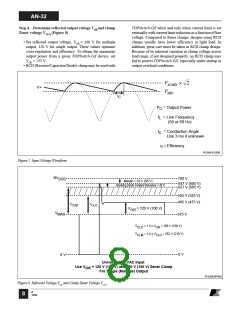
Step 23. Check BP ≤ 4200 . If necessary, reduce current
where IO is the output DC current
limit by lowering ILIMIT reduction factor KI
Step 28. Determine maximum peak inverse voltages PIVS,
PIVB for secondary and bias windings
ILIMIT(max)
•
BP =
× BM
IP
• Secondary winding maximum peak inverse voltage.
• Check BP ≤ 4200 gauss (0.42 tesla) to avoid transformer
saturation at startup and output over load.
• Decrease KI, if necessary, until BP ≤ 4200.
NS
PIV = VO + (VMAX
×
)
S
NP
• Bias winding maximum peak inverse voltage.
Step 24. Calculate secondary peak current ISP
NB
NP
PIVB = VB + (VMAX
×
)
•
ISP= IP ×
NP
NS
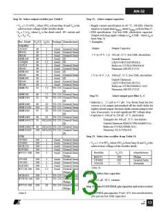
Step 29. Select clamp Zener and blocking diode per Table 8
for primary clamping based on VOR and the type of output
Step 25. Calculate secondary RMS current ISRMS
Blocking
Diode
BYV26C
MUR160 P6KE150
UF4005
Clamp
Zener
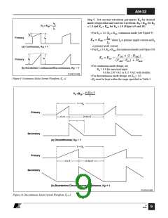
• Continuous mode
PS Output
VOR
2
KP
ISRMS = ISP × 1− D
×
− KP +1
(
)
MAX
Multiple Output 100 V
3
BYV26C
• Discontinuous mode
MUR160 P6KE180
UF4005
Single Output
120 V
1−DMAX
3 ×KP
ISRMS = ISP ×
Table 8.
B
12/02
12

 ETC [ ETC ]