AN-32
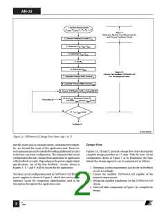
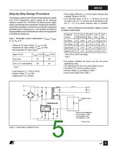
Step-by-Step Design Procedure
• Power supply efficiency, η: 0.8 if no better reference data
available. (Refer to AN-29)
ThisdesignprocedureusesthePIExpertdesignsoftware(available
from Power Integrations), which contains all the important
equations required for a TOPSwitch-GX flyback power supply
design,andautomatesmostcalculations.Designersare,therefore,
relievedfromthetediouscalculationsinvolvedinthecomplicated
and highly iterative design process. Look-up tables and empirical
designguidelinesareprovidedinthisprocedurewhereappropriate
to facilitate the design task.
• Loss allocation factor, Z: If Z = 1, all losses are on the
secondary side. If Z = 0, all losses are on the primary side.
Set Z = 0.5 if no better reference data is available.
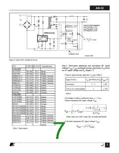
Step 2. Choose feedback circuit and bias voltage VB based
on output requirements
Feedback
Circuit
VB Circuit Load* Line
(V) Tolerance Reg. Reg.
Total
Reg.
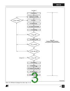
Step 1. Determine system requirements: VACMAX, VACMIN
,
fL, VO, PO, η, Z
Pri./Basic 5.8 ±10%
Pri./Enhan. 27.8 ±5%
±5% ±1.5% ±16.5%
±2.5% ±1.5% ±9%
±1% ±0.5% ±6.5%
±0.2% ±0.2% ±1.4%
• Minimum AC input voltage, VACMIN: in volts.
• Maximum AC input voltage, VACMAX: in volts.
• Recommended AC input ranges:
Opto/Zener 12
Opto/TL431 12
±5%
±1%
*Over 10% to 100% Load Range.
Table 2.
Input (VAC)
Universal
VACMIN (VAC) VACMAX (VAC)
85
265
265
• Use primary feedback for lowest cost (for low power
applications only).
230 or 115 with doubler
195
• Use Opto/Zener for low cost, good output accuracy.
• Use Opto/TL431 for best output accuracy.
• Set bias voltage VB according to Table 2.
• Choose optocoupler from Table 3.
Table 1.
• Line frequency, fL: 50 Hz or 60 Hz.
• Output voltage, VO: in Volts.
• Output power: PO: in Watts.
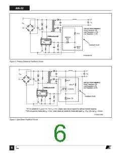
+
+
VO
-
VAC
CIN
Feedback Circuit
TOPSwitch-GX
15 Ω
D
S
L
CONTROL
C
X
F
CIRCUIT PERFORMANCE
Circuit Tolerance ±10%
Load Regulation ±5%
Line Regulation ±1.5%
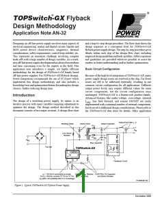
PI-3331-112202
Figure 3. Primary/Basic Feedback Circuit.
B
12/02
5

 ETC [ ETC ]