NT5DS32M4AT
NT5DS16M8AT
128Mb Double Data Rate SDRAM
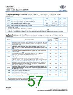
AC Input Operating Conditions (0 °C £ TA £ 70 °C; VDDQ = 2.5V ± 0.2V; VDD = 2.5V ± 0.2V, See AC
Characteristics)
Symbol
Parameter/Condition
Min
+ 0.31
REF
Max
Unit
V
Notes
1, 2
V
Input High (Logic 1) Voltage, DQ, DQS, and DM Signals
V
IH(AC)
V
V
Input Low (Logic 0) Voltage, DQ, DQS, and DM Signals
Input Differential Voltage, CK and CK Inputs
V
- 0.31
REF
V
V
V
1, 2
IL(AC)
0.62
V
+ 0.6
DDQ
1, 2, 3
1, 2, 4
ID(AC)
IX(AC)
V
Input Crossing Point Voltage, CK and CK Inputs
0.5*V
- 0.2 0.5*V
+ 0.2
DDQ
DDQ
1. Input slew rate = 1V/ns .
2. Inputs are not recognized as valid until V
stabilizes.
REF
3.
V
is the magnitude of the difference between the input level on CK and the input level on CK .
ID
4. The value of V is expected to equal 0.5*V
of the transmitting device and must track variations in the DC level of the same.
DDQ
IX
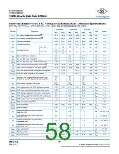
IDD Specifications and Conditions (0 °C £ TA £ 70 °C; VDDQ = 2.5V ± 0.2V; VDD = 2.5V ± 0.2V, See AC
Characteristics)
DDR266A/
DDR200
B
Symbol
Parameter/Condition
Unit
Notes
t
=10ns
CK
t
=7.5ns
CK
Operating Current: one bank; active / precharge; t = t
(min); DQ, DM, and
RC
RC
I
I
DQS inputs changing twice per clock cycle; address and control inputs changing
once per clock cycle
75
85
mA
mA
1
1
DD0
DD1
Operating Current: one bank; active / read / precharge; Burst = 2; t = t
RC
RC
(min); CL = 2.5; I
cycle
= 0mA; address and control inputs changing once per clock
90
110
OUT
Precharge Power-Down Standby Current: all banks idle; power-down mode;
I
I
I
15
30
15
15
35
15
mA
mA
mA
1
1
1
DD2P
DD2N
DD3P
CKE £ V (max)
IL
Idle Standby Current: CS ³ V (min); all banks idle; CKE ³ V (min);
IH
IH
address and control inputs changing once per clock cycle
Active Power-Down Standby Current: one bank active; power-down mode;
CKE £ V (max)
IL
Active Standby Current: one bank; active / precharge; CS ³ V (min);
IH
I
I
CKE ³ V (min); t
clock cycle; address and control inputs changing once per clock cycle
= t (max); DQ, DM, and DQS inputs changing twice per
50
60
mA
mA
mA
1
1
1
DD3N
DD4R
IH
RC
RAS
Operating Current: one bank; Burst = 2; reads; continuous burst; address and
control inputs changing once per clock cycle; DQ and DQS outputs changing
twice per clock cycle; CL = 2.5; I
130
115
165
150
= 0mA
OUT
Operating Current: one bank; Burst = 2; writes; continuous burst; address and
control inputs changing once per clock cycle; DQ and DQS inputs changing twice
per clock cycle; CL = 2.5
I
DD4W
I
Auto-Refresh Current: t
= t (min)
RFC
160
2
170
2
mA
mA
1
DD5
RC
I
Self-Refresh Current: CKE £ 0.2V
1, 2
DD6
Operating current: four bank; four bank interleaving with BL = 4, address and
control inputs randomly changing; 50% of data changing at every transfer;
t RC = t RC(min); I OUT = 0mA.
I
TBD
TBD
mA
1
DD7
1. I
specifications are tested after the device is properly initialized.
DD
2. Enables on-chip refresh and address counters.
57
REV 1.0
May, 2001
©
NANYA TECHNOLOGY CORP. All rights reserved.
NANYA TECHNOLOGY CORP. reserves the right to change Products and Specifications without notice.

 ETC [ ETC ]