NT5DS32M4AT
NT5DS16M8AT
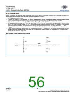
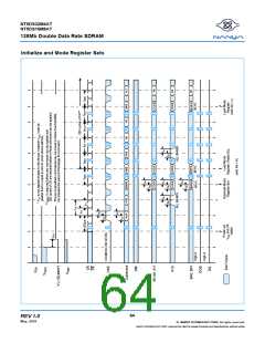
128Mb Double Data Rate SDRAM
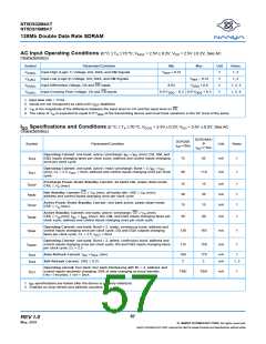
Electrical Characteristics & AC Timing for DDR266DDR200 - Applicable Specifications
Expressed in Clock Cycles (0 °C £ TA £ 70 °C; VDDQ = 2.5V ± 0.2V; VDD = 2.5V ± 0.2V, See AC Characteristics)
t
= 7.5ns
CK
Symbol
Parameter
Units
Notes
Min
2
Max
t
Mode register set command cycle time
t
t
t
t
1-4
1-4
1-4
1-4
MRD
CK
CK
CK
CK
t
Write preamble
0.25
6
WPRE
t
Active to Precharge command
Active to Active/Auto-refresh command period
16000
RAS
t
9
RC
Auto-refresh to Active/Auto-refresh
command period
t
10
t
1-4
RFC
CK
t
t
Active to Read or Write delay
3
3
t
t
t
t
t
t
t
t
t
1-4
1-4
1-4
1-4
1-4
1-5
1-4
1-4
1-4
RCD
RAP
CK
CK
CK
CK
CK
CK
CK
CK
CK
Active to Read Command with Autoprecharge
Precharge command period
t
3
RP
t
Active bank A to Active bank B command
Write recovery time
2
RRD
t
2
WR
t
Auto precharge write recovery + precharge time
Internal write to read command delay
Exit self-refresh to non-read command
Exit self-refresh to read command
5
DAL
t
1
WTR
t
10
200
XSNR
XSRD
t
1. Input slew rate = 1V/ns
2. The CK/CK input reference level (for timing reference to CK/CK) is the point at which CK and CK cross: the input reference level for sig-
nals other than CK/CK , is V
REF.
3. Inputs are not recognized as valid until V
stabilizes.
REF
4. The Output timing reference level, as measured at the timing reference point indicated in AC Characteristics (Note 3) is V
.
TT
5.
t
and t transitions occur in the same access time windows as valid data transitions. These parameters are not referred to a specific
HZ LZ
voltage level, but specify when the device is no longer driving (HZ), or begins driving (LZ).
60
REV 1.0
May, 2001
©
NANYA TECHNOLOGY CORP. All rights reserved.
NANYA TECHNOLOGY CORP. reserves the right to change Products and Specifications without notice.

 ETC [ ETC ]