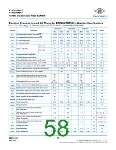
NT5DS32M4AT
NT5DS16M8AT
128Mb Double Data Rate SDRAM
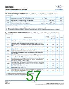
Electrical Characteristics & AC Timing for DDR266/DDR200 - Absolute Specifications
(0 °C £ TA £ 70 °C; VDDQ = 2.5V ± 0.2V; VDD = 2.5V ± 0.2V, See AC Characteristics) (Part 1 of 2)
DDR266A
DDR266B
DDR200
Symbol
Parameter
Unit
Notes
Min
Max
Min
Max
Min
Max
+ 0.8
+ 0.8
t
DQ output access time from CK/CK
DQS output access time from CK/CK
CK high-level width
- 0.75
- 0.75
0.45
0.45
7
+ 0.75
+ 0.75
- 0.75
- 0.75
0.45
+ 0.75
+ 0.75
- 0.8
- 0.8
0.45
0.45
8
ns
ns
1-4
1-4
1-4
1-4
1-4
AC
t
DQSCK
t
0.55
0.55
12
0.55
0.55
12
0.55
0.55
12
t
t
CH
CK
CK
t
CK low-level width
0.45
CL
t
CL = 2.5
7.5
ns
CK
Clock cycle time
7.5
12
t
CL = 2.0
10
12
10
12
ns
1-4
CK
10
12
t
t
DQ and DM input hold time
DQ and DM input setup time
0.5
0.5
0.5
0.6
0.6
ns
ns
ns
ns
ns
ns
ns
1-4
1-4
DH
DS
0.5
t
DQ and DM input pulse width (each input)
Data-out high-impedance time from CK/CK
Data-out low-impedance time from CK/CK
DQS-DQ skew (DQS & associated DQ signals)
DQS-DQ skew (DQS & all DQ signals)
1.75
- 0.75
- 0.75
1.75
2
1-4
DIPW
t
+ 0.75
+ 0.75
+ 0.5
- 0.75
- 0.75
+ 0.75
+ 0.75
+ 0.5
- 0.8
- 0.8
+ 0.8
+ 0.8
+ 0.6
+ 0.6
1-4, 5
1-4, 5
1-4
HZ
t
LZ
t
DQSQ
t
+ 0.5
+ 0.5
1-4
DQSQA
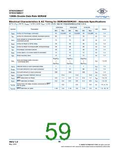
t
t
t
t
t
CH
or
CH
or
CH
or
minimum half clk period for any given cycle;
t
t
t
1-4
1-4
HP
QH
CK
CK
defined by clk high (t ) or clk low (t ) time
CH
CL
t
CL
CL
CL
t
-
t
-
t
HP
-
HP
HP
Data output hold time from DQS
t
0.75ns
0.75
0.35
0.2
0.75ns
0.75
0.35
0.2
1.0ns
0.75
0.35
0.2
t
Write command to 1st DQS latching transition
DQS input low (high) pulse width (write cycle)
DQS falling edge to CK setup time (write cycle)
DQS falling edge hold time from CK (write cycle)
Mode register set command cycle time
Write preamble setup time
1.25
1.25
1.25
t
t
t
t
1-4
1-4
DQSS
CK
CK
CK
CK
t
DQSL,H
t
1-4
DSS
t
0.2
0.2
0.2
1-4
DSH
t
14
15
16
ns
ns
1-4
MRD
t
0
0
0
1-4, 7
1-4, 6
1-4
WPRES
t
Write postamble
0.40
0.25
0.60
0.40
0.25
0.60
0.40
0.25
0.60
t
WPST
CK
CK
t
Write preamble
t
WPRE
Address and control input hold time
(fast slew rate)
t
0.9
0.9
1.0
1.0
0.9
0.9
1.0
1.0
1.1
1.1
1.1
1.1
ns
ns
ns
2-4, 11,13,14
2-4, 11,13,14
2-4, 12-14
IH
Address and control input setup time
(fast slew rate)
t
IS
Address and control input hold time
(slow slew rate)
t
t
IH
IS
Address and control input setup time
(slow slew rate)
ns
ns
2-4, 12-14
t
Input pulse width
Read preamble
Read postamble
2.2
0.9
2.2
0.9
2-4, 14
1-4
IPW
t
1.1
1.1
0.9
1.1
t
RPRE
CK
CK
t
0.40
0.60
0.40
0.60
0.40
0.60
t
1-4
RPST
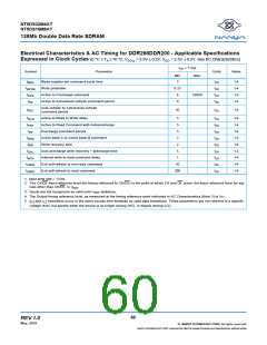
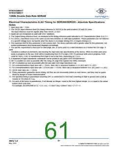
58
REV 1.0
May, 2001
©
NANYA TECHNOLOGY CORP. All rights reserved.
NANYA TECHNOLOGY CORP. reserves the right to change Products and Specifications without notice.

 ETC [ ETC ]