Applications
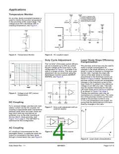
Temperature Monitor
VCC
VCC
L1 and L3 = Siemens Chip
Inductors (B82432A1224K).
L2 and L4 = Siemens ferrite
cores B64290-A36-X33 with
8 turns of 0.22mm Cu-Wire.
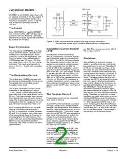
An on-chip, diode connected transistor is
used to monitor the junction temperature
in the proximity of the output stage. The
voltage at pin MTJ decreases with in-
creasing temperature, see Figure 4.
L1
220uH
L3
220uH
VCC
VCC
L2
L4
VCC
25W
25W
2k
100nF
IMB
IM
MTJ
100nF
IB
L
VEE
Figure 4. Temperature Monitor.
Figure 6. AC coupled output.
Duty Cycle Adjustment
Laser Diode Slope Efficiency
Compensation
1. 00V
The “on-time” of the laser current (IM-pin)
can be increased up to 20% by control-
ling the voltage at the Duty input. In the
configuration in Figure 7, a smaller R re-
sults in a longer on-time. The duty cycle
adjustment can be monitored using the
Mark/Space monitor outputs (MARKP/
MARKN), see Figure 8.
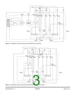
The pre-bias control loop may be used to
make a simple compensation for
changes in the slope efficiency of a laser
diode, in order to maintain a constant ex-
tinction ratio. Typically the slope effi-
ciency of the laser diode is inversely
proportional to the threshold current, as
shown in Figure 9 below. Therefore the
pre-bias monitor current will compensate
changes in the threshold current of the
laser diode if it is added to the reference
voltage on pin IMC at a ratio. This ratio
may be chosen individually for the spe-
cific laser diode and is set by an external
R as shown in Figure 3 on page 3.
Thereby the extinction ratio may be
maintained at a constant ratio. The varia-
tion of the pre-bias monitor current com-
pared to the pre-bias current is only
+/-1% over temperature and supply, en-
suring that the performance is not sacri-
ficed by changes in this ratio.
0. 90V
0. 80V
0. 75V
VCC
VCC
- 30
0
50
100
130
TEMP
1k
DUTY
R
Figure 5. Voltage at pin MTJ versus
Temperature.
DC Coupling
VEE
VEE
VEE
For a compact design, pre-bias and mod-
ulation current can be DC coupled. DC
coupling is appropriate when connections
between laser driver and laser diode are
kept short (with low inductance) as
achieved, e.g. by flip-chip mounting of
the two dice in close proximity, see
Figure 10 on page 5. The GD16521 is
optimized for this configuration.
Figure 7. Duty cycle adjustment with an
external resistor.
P
O
MARKP
100nF
MARKP
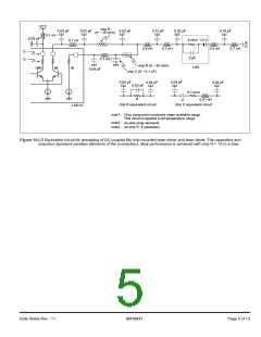
AC Coupling
AC coupling is recommended for the
packaged version, in particular when the
output is connected to the laser diode
through a transmission line, see Figure 6.
Figure 8. MARKP/MARKN outputs.
I
L
Figure 9. Laser diode characteristics
Data Sheet Rev.: 11
GD16521
Page 4 of 13

 ETC [ ETC ]