CML Input
Functional Details
VCC
100nF TDIP
GD16521 is a 2.5 Gbit/s laser driver with
an optional re-timing of the data signal. It
is capable of driving laser diodes, at a
maximum modulation current of 50 mA
and a maximum pre-bias current of
100 mA.
VCC
500W
50W
1kW
50W
50W
50W
50W
100nF SDIP
100nF SDIN
1kW
The Inputs
100nF
TDIN
VEE
50W
1kW
Data (SDIP/SDIN) is input to GD16521
and re-timed within a DFF clocked by an
external clock (SCIP/SCIN). Optionally
the re-timing may be bypassed controlled
by a select pin (FFSET).
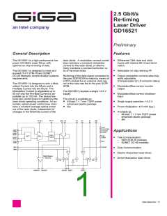
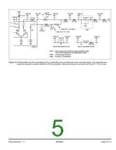
Figure 1. CML input termination scheme with loop through connection.
This example shows an AC coupled differential input configuration.
Input Termination
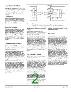
Modulation Current Control
Loop
pin IBM. The mirrored current is 1/20 of
the pre-bias current.
The data inputs (SDIP/SDIN) and clock
inputs (SCIP/SCIN)are internally termi-
nated to 50 W through the pins TDIP/
TDIN and TCIP/TCIN respectively, see
Figure 1 below. Using this scheme a
VSWR better than 1.5 up to 1.75 GHz
and better than 2 up to 2.5 GHz can be
achieved. The inputs are internally bi-
ased to 2×(VCC - VEE )/3 with a resistive
divider.
A modulation current control loop
(MCCL) maintaining a constant modula-
tion current has been incorporated into
GD16521. The MCCL OP-amp controls
the modulation current so that the volt-
age across an external resistor caused
by the current sink into the IMM pin
which is 1/20 of the modulation current
equals an external reference voltage ap-
plied to the IMC pin. The voltage applied
to the IMC pin sets the modulation cur-
rent. Because the sink current into the
IMM pin is 1/20 of the modulation current
sink into pin IM the MCCL maintains a
constant modulation current. Loop stabi-
lity is obtained by adding an external ca-
pacitor across the OP-amp, see Figure 2
below.
Shutdown
Also added is an anti-rush circuitry,
which is used to avoid over loading the
laser diode during turn on. Typically AR
or PD are connected, see Figure 2. In
this case, the bias and modulation cur-
rent are turned off, there will not be any
voltage across the resistor connected to
the back facet monitor diode photo de-
tector. Therefore, without the anti-rush
circuitry, the OPCL will adjust to increase
the bias current, effectively setting the
bias control voltage to its maximum, re-
gardless of the setting of the voltage on
the OPSET pin. Once the bias and
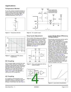
The Modulation Current
The output pins (IM/IMB) are open col-
lector outputs designed for driving an ex-
ternal load with a controlled current,
typically a laser diode.
The output modulation current can be
controlled in the range from 0 mA to
70 mA. The AC specifications are how-
ever valid only in the range from 9 mA to
50 mA. The output voltage swing across
the external load may be varied accord-
ingly. The external load however must be
designed so that the voltage on the out-
put will never be lower than VCC -2 V.
modulation current is turned on again,
the laser diode will be subject to the full
bias current, and this may harm the laser
diode. Therefore, an anti-rush circuitry
has been provided, which sinks a current
into the AR/PD pins when the bias and
modulation current is turned off, SHDW =
“1”. This causes the AR/PD pins to be-
come more negative than the reference
voltage on the OPSET pin, and therefore
causes the OPCL to turn down the con-
trol for the bias current. This ensures a
smooth turn on of the laser diode.
The Pre-bias Current
The pre-bias current can be controlled
from 0 mA to 100 mA.
A control loop that maintains a constant
average optical power, independent of
changes over temperature and lifetime in
the laser diode threshold current is incor-
porated in GD16521. The optical power
control loop (OPCL) OP-amp adjusts the
laser diode pre-bias current so that the
voltage drop across the resistor con-
nected to the back facet monitor diode
photo detector, applied to the PD pin,
equals the voltage applied to the OPSET
pin, see Figure 2 below.
In AC coupling the circuit can be oper-
ated at modulation currents above
50 mA. At modulation currents between
50 and 70 mA together with a high oper-
ating temperature, there is, however, a
small penalty in AC performance. The
output jitter can exceed the specification,
fall times can exceed the specified
values by 10% while rise time are within
specifications.
The voltage applied to the OPSET pin
determines the average optical power.
Loop stability is obtained by adding an
external capacitor across the OP-amp.
In addition to the modulation current con-
trol and the pre-bias control loops de-
scribed above, GD16521 features a
current mirror of the bias current on the
Data Sheet Rev.: 11
GD16521
Page 2 of 13

 ETC [ ETC ]