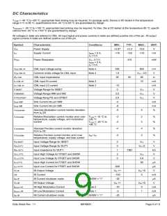
DC Characteristics
TCASE = -40 °C to +95 °C, appropriate heat sinking may be required, for package parts. Device is DC-tested in the temperature
range 0 °C to 85 °C, specifications from -40 °C to 95 °C are guaranteed by design.
TDIE BACK = -30 °C to +100 °C, appropriate heat sinking may be required, for dies. Die is DC-tested at the temperature 85 °C, specifi-
cations from -30 °C to +100 °C are guaranteed by design.
All voltages in table are referred to VEE. All input signal and power currents in table are defined positive into of the pin. All output
signal currents in table are defined positive out of the pin.
Symbol:
VCC
Characteristic:
Power Supply
Supply Current
Conditions:
MIN.:
+2.97
-170
TYP.:
+3.3
MAX.:
+3.6
UNIT:
V
ICC
IIM/IMB = 0 A,
IIB = 0 A
-125
-110
mA
PDISS
Power Dissipation
VCC = 3.3 V,
410
mW
IIM/IMB = 0 A,
IIB = 0 A
VDiff CML IN
VCM CML IN
ZIN CML
CML input voltage swing.
Common mode voltage for CML input.
CML input impendance
Note 4
Note 4
300
1.8
35
800
VCC - 0.5
65
mV
V
50
W
IHI CML IN
ILO CML IN
V IMSET
CML input HI current
Note 3
Note 3
10
mA
mA
V
CML input LO current
-10
0
Voltage Range for IMSET
Voltage Range IMM and IMC
Voltage Rang PD and OPSET
Sink Current into pin IMM
Sink Current into pin IMB
VCC
VCC
VCC
V IMM/IMC
V PD/OPSET
ISINK IMM
2.5
2.5
-4
V
V
mA
mA
%
ISINK IMB
-8
D ABSIM/IMM
Absolute Modulation current monitor deviation
from IIM /20
-5
5
D RELIB/IBM
Relative Modulation current monitor error over
temperature, supply voltage, and modulation
current
T
CASE = -10 °C to
+95 °C
CASE = -40 °C to
+95 °C
-2
-3
2
3
%
%
T
D ABSIB/IBM
Absolute Pre-bias current monitor deviation
from IIB /20
-4
-2
4
2
%
%
D RELIB/IBM
Relative Pre-bias current monitor error over
temperature, supply voltage, and bias current
IIBM / IIM
VIN IBSET
VIN DUTY
RIN DUTY
VHI LVTTL
VLO LVTTL
IHI LVTTL
ILO LVTTL
VO IB
Input Voltage Range for IBSET
Input Voltage Range for DUTY
Input impedance for DUTY
Input High Voltage for FFSET and SHDW
Input Low Voltage for FFSET and SHDW
Input High Current for FFSET and SHDW
Input Low Current for FFSET and SHDW
IB Output Voltage
0
0
1
2
0
VCC
V
V
VCC /2
TBD
kW
V
VCC
0.8
50
V
mA
mA
V
-500
VEE +1
- 100
- 25
VEE +5
I IB
IB Current
0
mA
mA
V
ISD IB
IB Current shutdown mode
IM Output Voltage
SHDW = “1"
VO IM
VEE +1
- 70
VEE +5
IMod,HI IM
IMod,LO IM
ISD IM
IM High Modulation Current
IM Low Modulation Current
IM Current shutdown mode
Note 2
0
1
mA
mA
mA
Note 1
- 3
SHDW = “1"
- 25
Data Sheet Rev.: 11
GD16521
Page 9 of 13

 ETC [ ETC ]