July 2004
AS91L1006BU
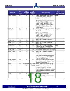
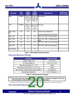
PIN
NUMBER NUMBER
LQFP FPBGA
PIN
PIN
TYPE
Stable state
after port/reset
PIN NAME
DESCRIPTION
GND
POWER 38, 86, 11, D6, G5, C3, Ground pins.
26, 43, 59, D7, E5, F6,
74, 95, 2, G4,H8, H9,
17, 54, 55 J9,B1, A5,
90
F2
VCC
POWER
IN
39, 91, 3, D5, G6, C8, VCC pins.
18, 34, 51, D4, E6, F5,
66,
G7,
82,23,56 H3,G9,H1
ASIC_TEST_
EN
89
B5
Factory Test_Enable Input.
This pin should be left unconnected.
IEEE1149.1 ASIC Test Clock Input.
ASIC_TCK
ASIC_TMS
ASIC_TDO
IN
IN
62
15
73
F8
F3
IEEE1149.1 ASIC Test Mode Select.
Input
IEEE1149.1 ASIC Test Clock Output.
OUT
A10
ASIC_TDI
IN
4
1
A1
C1
IEEE1149.1 ASIC Test Clock Input.
No Connects
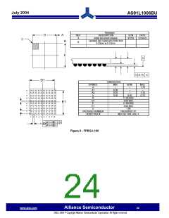
Table 9 - AS91L0006BU Signal Description
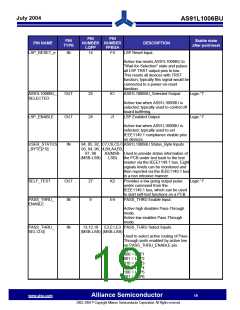
Absolute Maximum Ratings
Parameter
Supply Voltage (Vcc)
Maximum Range
-0.3V to 5.5V
DC Input Voltage (Vi)
-0.5V to Vcc +0.5V
-20mA
Max sink current when Vi = -0.5V
Max source current when Vi = Vcc + 0.5V
Max Junction Temperature with power applied Tj
Max Storage temperature
+20mA
+125 degrees C
-55 to +150 degree C
Table 10 - Absolute Maximum Ratings
ꢁNote: Stress above the stated maximum values may cause irreparable damage to the device.
Correct operation of the device at these values is not guaranteed.
Recommended Operating Conditions
www.alsc.com
Alliance Semiconductor
2003, 2004 © Copyright Alliance Semiconductor Corporation. All Rights reserved.
20

 ETC [ ETC ]