<ꢀ5ꢁꢀꢂꢃ<ꢀ.ꢁꢀꢂ
'PJCPEGFꢄ<ꢁꢀꢂꢄ/KETQRTQEGUUQT
ZiLOG
12'4#6+10ꢄ/1&'5
<ꢀꢂꢄXGTUWUꢄꢈꢉꢁꢀꢂꢄ%QORCVKDKNKV[ꢆꢄThe Z8S180/Z8L180
is descended from two different “ancestor” processors,
ZiLOG’s original Z80 and the Hitachi 64180. The Operat-
ing Mode Control Register (OMCR), illustrated in Figure
8, can be programmed to select between certain Z80 and
64180 differences.
/ꢁ'ꢄꢌ/ꢁꢄ'PCDNGꢍꢆꢄThis bit controls the /ꢄ output and is
set to a 1 during 4'5'6.
When /ꢄ'ꢅꢐꢅ1, the /ꢄ output is asserted Low during op-
code fetch cycles, Interrupt Acknowledge cycles, and the
first machine cycle of an 0/+ acknowledge.
On the Z8S180/Z8L180, this choice makes the processor
fetch a 4'6+ instruction one time. When fetching a 4'6+
from a zero-wait-state memory location, the processor uses
three clock bus cycles. These bus cycles are not fully Z80-
timing compatible.
&ꢊ &ꢁ &ꢏ
4GUGTXGF
+1%ꢅꢈ4ꢌ9ꢉ
/ꢄ6'ꢅꢈ9ꢉ
/ꢄ'ꢅꢈ4ꢌ9ꢉ
When /ꢄ' ꢐ 0, the processor does not drive /ꢄ Low dur-
ing the instruction fetch cycles. After fetching a 4'6+ in-
struction with normal timing, the processor goes back and
refetches the instruction using fully Z80-compatible cycles
that include driving /ꢄ Low. This option may be required
by some external Z80 peripherals to properly decode the
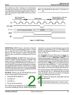
4'6+ instruction. Figure 9 and Table 5 show the 4'6+ se-
quence when /ꢄ' is 0.
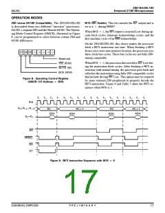
(KIWTG ꢀꢆ 1RGTCVKPIꢄ%QPVTQNꢄ4GIKUVGT
ꢌ1/%4ꢅꢄ+ꢃ1ꢄ#FFTGUUꢄꢒꢄꢋ'*ꢍ
6
6
6
6
6
6
6
6
6
6
6
6
6
6
6
6
6
2*+
ꢅꢈ#
#
#
ꢉ
2%ꢔꢄ
2%
'&*
2%ꢔꢄ
ꢎ&*
2%
'&*
ꢎ&*
&
&
/ꢄ
/4'3
4&
56
(KIWTG ꢏꢆ 4'6+ꢄ+PUVTWEVKQPꢄ5GSWGPEGꢄYKVJꢄ/ꢁ'ꢄꢒꢄꢂ
&5ꢀꢀꢁꢀꢀꢂꢃ</2ꢀꢂꢀꢀ
2ꢅ4ꢅ'ꢅ.ꢅ+ꢅ/ꢅ+ꢅ0ꢅ#ꢅ4ꢅ;
ꢄꢊ

 ZILOG [ ZILOG, INC. ]