eZ80L92 MCU
Product Specification
184
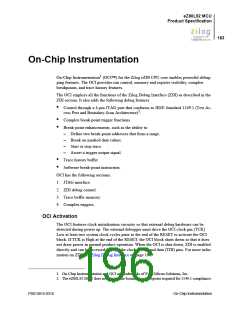
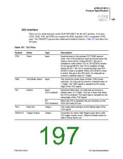
OCI Interface
There are five dedicated pins on the ZLP12840 MCU for the OCI interface. Four pins
(TCK, TMS, TDI, and TDO) are required for IEEE Standard 1149.1-compatible JTAG
ports. The TRIGOUT pin provides additional testability features. Table 107 lists these five
OCI pins.
Table 107. OCI Pins
Symbol
Name
Type
Description
TCK
Clock.
Input
Asynchronous to the primary ZLP12840 system
clock. The TCK period but must be at least twice the
system clock period. During RESET, this pin is
sampled to select either OCI or ZDI DEBUG modes.
If Low during RESET, the OCI is enabled. If High
during RESET, the OCI is powered down and ZDI
DEBUG mode is enabled. When ZDI DEBUG mode
is active, this pin is the ZDI clock. On-chip pull-up
ensures a default value of 1 (High).
TMS
TDI
Test Mode Select Input
This serial test mode input controls JTAG mode
selection. On-chip pull-up ensures a default value of
1 (High). The TMS signal is sampled on the rising
edge of the TCK signal.
Data In
Input
Serial test data input. On-chip pull-up ensures a
default value of 1 (High). This pin is input-only when
the OCI is enabled. The input data is sampled on the
rising edge of the TCK signal.
(OCI enabled)
I/O
When the OCI is disabled, this pin functions as the
(OCI disabled) ZDA (ZDI Data) I/O pin.
TDO
Data Out
Output
The output data changes on the falling edge of the
TCK signal.
TRIGOUT Trigger Output
Output
Generates an active High trigger pulse when valid
OCI trigger events occur. Output is tristate when no
data is being driven out.
PS013015-0316
On-Chip Instrumentation

 ZILOG [ ZILOG, INC. ]