eZ80L92 MCU
Product Specification
162
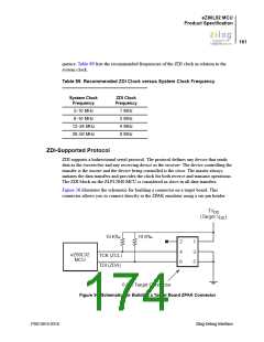
ZDI Clock and Data Conventions
The two pins used for communication with the ZDI block are ZDI Clock pin (ZCL) and
ZDI Data pin (ZDA). On ZLP12840 MCU, the ZCL pin is shared with the TCK pin while
the ZDA pin is shared with the TDI pin. The ZCL pin and ZDA pin functions are only
available when the on-chip instrumentation is disabled and the ZDI is therefore enabled.
For general data communication, the data value on the ZDA pin changes only when ZCL
is Low (0). The only exception is the ZDI START bit, which is indicated by a High-to-
Low transition (falling edge) on the ZDA pin while ZCL is High.
Data is shifted in and out of ZDI, with the most significant bit (bit 7) of each byte being
first in time, and the least significant bit (bit 0) last in time. The information is transferred
between the master and the slave in 8-bit (single-byte) units. Each byte is transferred with
nine clock cycles: eight to shift the data, and the ninth for internal operations.
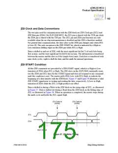
ZDI START Condition
All the ZDI commands are preceded by a ZDI START signal, which is a High-to-Low
transition of ZDA when ZCL is High. The ZDI slave on the ZLP12840 continually moni-
tors the ZDA and ZCL lines for the START signal and does not respond to any command
until this condition is met. The master pulls ZDA Low, with ZCL High, to indicate the
beginning of a data transfer with the ZDI block. Figure 37 and Figure 38 illustrate a valid
ZDI START signal prior to writing and reading the data, respectively. A Low-to-High
transition of ZDA while the ZCL is High produces no effect.
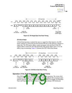
Data is shifted in during a Write to the ZDI block on the rising edge of ZCL, as illustrated
in Figure 37. Data is shifted out during a Read from the ZDI block on the falling edge of
ZCL as illustrated in Figure 38. When an operation is completed, the master stops during
the ninth cycle and holds the ZCL signal High.
ZDI Data In
(Write)
ZDI Data In
(Write)
ZCL
ZDA
Start Signal
Figure 37. ZDI Write Timing
PS013015-0316
Zilog Debug Interface

 ZILOG [ ZILOG, INC. ]