MVTX2801
Data Sheet
Bit[3]
(Default 1'B0)
Polarity control of led_byteout_[6]
0: not invert
1: invert
Bit [2:0] (Default 3'b001)
Signal Select:
0: not select
1: select the corresponding bit
When bits get selected, the led_byteout_[0] = OR (all selected bits)
10.7.21 MIINP0 - MII Next Page Data Register 0
2
I C Address:h0C3, Serial Interface Address:h614
Access by CPU and serial interface only (R/W)
Bit [7:0]
MII next page Data [7:0]
10.7.22 MIINP1 - MII Next Page Data Register 1
2
I C Address:h0C4, Serial Interface Address:h615
Access by CPU and serial interface only (R/W)
Bit [7:0]
MII next page Data [15:8]
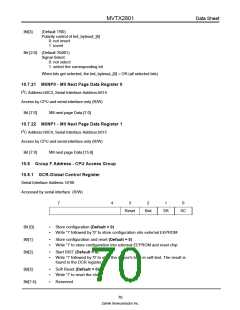
10.8 Group F Address - CPU Access Group
10.8.1 GCR-Global Control Register
Serial Interface Address: hF00
Accessed by serial interface. (R/W)
7
4
3
2
1
0
Reset
Bist
SR
SC
Bit [0]:
Bit[1]:
Bit[2]:
•
•
Store configuration (Default = 0)
Write '1' followed by '0' to store configuration into external EEPROM
•
•
Store configuration and reset (Default = 0)
Write '1' to store configuration into external EEPROM and reset chip
•
•
Start BIST (Default = 0)
Write '1' followed by '0' to start the device's built-in self-test. The result is
found in the DCR register.
Bit[3]:
•
•
Soft Reset (Default = 0)
Write '1' to reset the chip
Bit[7:4]:
•
Reserved
70
Zarlink Semiconductor Inc.

 ZARLINK [ ZARLINK SEMICONDUCTOR INC ]