MT88L70
Data Sheet
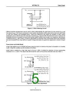
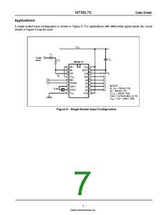
Differential Input Configuration
The input arrangement of the MT88L70 provides a differential-input operational amplifier as well as a bias source
(VRef) which is used to bias the inputs at mid-rail. Provision is made for connection of a feedback resistor to the op-
amp output (GS) for adjustment of gain. In a single-ended configuration, the input pins are connected as shown in
Figure 6 with the op-amp connected for unity gain and VRef biasing the input at 1/2VDD. Figure 5 shows the
differential configuration, which permits the adjustment of gain with the feedback resistor R5.
MT88L70
R1
IN+
IN-
C1
+
-
C2
R4
GS
R3
R5
R2
VRef
DIFFERNTIAL INPUT AMPLIFIER
C1 = C2 = 10 nF
All resistors are ± 1% tolerance.
All capacitors are ± 5% tolerance.
R1 = R4 = R5 = 100 kΩ
R2 = 60 kΩ, R3, = 37.5 kΩ
R2R5
R2 + R5
R3 =
R5
R1
VOLTAGE GAIN (AV diff) =
INPUT IMPEDANCE
2
1
ωC
2
R1
+
(ZINDIFF) = 2
Figure 5 - Differential Input Configuration
Crystal Oscillator
The internal clock circuit is completed with the addition of an external 3.579545 MHz crystal and is connected as
shown in Figure 6 (Single-ended Input Configuration).
6
Zarlink Semiconductor Inc.

 ZARLINK [ ZARLINK SEMICONDUCTOR INC ]