MT88L70
Data Sheet
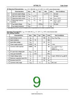
18
17
16
15
14
13
12
11
10
1
2
20
19
18
17
16
15
14
13
12
11
1
2
IN+
IN-
VDD
St/GT
ESt
StD
Q4
IN+
IN-
VDD
St/GT
ESt
StD
NC
GS
3
4
5
3
4
5
GS
VRef
INH
VRef
INH
PWDN
6
7
8
9
Q3
PWDN
NC
6
7
Q4
Q2
OSC1
OSC2
VSS
Q3
Q1
OSC1
OSC2
VSS
8
Q2
TOE
9
Q1
10
TOE
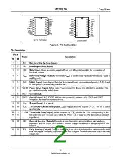
18 PIN PDIP/SOIC
20 PIN SSOP
Figure 2 - Pin Connections
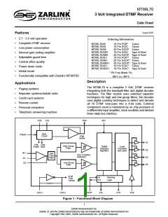
Description
Pin Description
Pin #
Name
18 20
1
2
3
1
2
3
IN+
IN-
GS
Non-Inverting Op-Amp (Input).
Inverting Op-Amp (Input).
Gain Select. Gives access to output of front end differential amplifier for connection of
feedback resistor.
4
5
6
4
5
6
VRef Reference Voltage (Output). Nominally VDD/2 is used to bias inputs at mid-rail (see Figure 5
and Figure 6).
INH
Inhibit (Input). Logic high inhibits the detection of tones representing characters A, B, C and
D. This pin input is internally pulled down.
PWDN Power Down (Input). Active high. Powers down the device and inhibits the oscillator. This
pin input is internally pulled down.
7
8
8
9
OSC1 Clock (Input).
OSC2 Clock (Output). A 3.579545 MHz crystal connected between pins OSC1 and OSC2
completes the internal oscillator circuit.
9
10
VSS
Ground (Input). 0 V typical.
10 11
TOE Three State Output Enable (Input). Logic high enables the outputs Q1-Q4. This pin is pulled
up internally.
11- 12- Q1-Q4 Three State Data (Output). When enabled by TOE, provide the code corresponding to the
14 15
last valid tone-pair received (see Table 1). When TOE is logic low, the data outputs are high
impedance.
15 17
StD
ESt
Delayed Steering (Output).Presents a logic high when a received tone-pair has been
registered and the output latch updated; returns to logic low when the voltage on St/GT falls
below VTSt
.
16 18
Early Steering (Output). Presents a logic high once the digital algorithm has detected a valid
tone pair (signal condition). Any momentary loss of signal condition will cause ESt to return to
a logic low.
2
Zarlink Semiconductor Inc.

 ZARLINK [ ZARLINK SEMICONDUCTOR INC ]