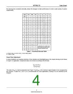
MT88L70
Data Sheet
Absolute Maximum Ratings†
Parameter
DC Power Supply Voltage
Symbol
Min.
Max.
Units
1
2
3
4
5
VDD
VI
7
V
Voltage on any pin
VSS-0.3
-65
VDD+0.3
10
V
Current at any pin (other than supply)
Storage temperature
II
mA
°C
TSTG
PD
+150
500
Package power dissipation
mW
† Exceeding these values may cause permanent damage. Functional operation under these conditions is not implied.
Derate above 75 °C at 16 mW / °C. All leads soldered to board.
Recommended Operating Conditions - Voltages are with respect to ground (VSS) unless otherwise stated.
Parameter
Sym. Min.
Typ.‡
Max. Units
Test Conditions
1
2
3
4
DC Power Supply Voltage
Operating Temperature
VDD
TO
fc
2.7
-40
3.0
3.6
V
°C
+85
Crystal/Clock Frequency
3.579545
MHz
Crystal/Clock Freq.Tolerance
‡ Typical figures are at 25°C and are for design aid only: not guaranteed and not subject to production testing.
∆fc
±0.1
%
DC Electrical Characteristics - VDD = 3.0 V+ 20%/-10%, VSS = 0 V, -40°C ≤ TO ≤ +85°C, unless otherwise stated.
Characteristics
Sym.
Min.
Typ.‡
Max.
Units
Test Conditions
PWDN=VDD
S
U
P
P
L
1
2
3
Standby supply current
Operating supply current
Power consumption
IDDQ
IDD
1
2.0
6
10
µA
5.5
mA
PO
mW fc=3.579545 MHz
Y
4
5
6
7
High level input
VIH
VIL
2.1
V
V
VDD = 3.0 V
Low level input voltage
Input leakage current
Pull up (source) current
0.9
5
VDD = 3.0 V
IIH/IIL
ISO
0.05
4
µA
µA
VIN = VSS or VDD
TOE (pin 10) = 0,
I
N
P
U
T
S
15
V
DD = 3.0 V
8
Pull down (sink) current
ISI
15
40
µA
INH = VDD, PWDN =
VDD, VDD = 3.0 V
9
Input impedance (IN+, IN-)
Steering threshold voltage
RIN
10
MΩ
@ 1 kHz
10
VTSt
0.465VDD
V
8
Zarlink Semiconductor Inc.

 ZARLINK [ ZARLINK SEMICONDUCTOR INC ]