MT88L70
Data Sheet
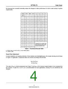
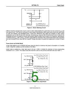
VDD
C
VDD
vc
St/GT
ESt
R
StD
tGTA=(RC)In(VDD/VTSt
)
MT88L70
tGTP=(RC)In[VDD/(VDD-VTSt)]
Figure 3 - Basic Steering Circuit
Different steering arrangements may be used to select independently the guard times for tone present (tGTP) and
tone absent (tGTA). This may be necessary to meet system specifications which place both accept and reject limits
on both tone duration and interdigital pause. Guard time adjustment also allows the designer to tailor system
parameters such as talk off and noise immunity. Increasing tREC improves talk-off performance since it reduces the
probability that tones simulated by speech will maintain signal condition long enough to be registered. Alternatively,
a relatively short tREC with a long tDO would be appropriate for extremely noisy environments where fast acquisition
time and immunity to tone drop-outs are required. Design information for guard time adjustment is shown in Figure
4.
Power-down and Inhibit Mode
A logic high applied to pin 6 (PWDN) will power down the device to minimize the power consumption in a standby
mode. It stops the oscillator and the functions of the filters.
Inhibit mode is enabled by a logic high input to the pin 5 (INH). It inhibits the detection of tones representing
characters A, B, C, and D. The output code will remain the same as the previous detected code (see Table 1).
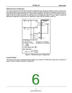
t
GTP=(RPC1) In [VDD / (VDD-VTSt)]
tGTA=(R1C1) In (VDD / VTSt
RP = (R1R2) / (R1 + R2)
VDD
)
C1
St/GT
R1
R2
ESt
a) decreasing tGTP; (tGTP < tGTA
GTP=(R1C1) In [VDD / (VDD-VTSt)]
tGTA=(RPC1) In (VDD / VTSt
)
t
VDD
)
C1
RP = (R1R2) / (R1 + R2)
St/GT
R2
R1
ESt
b) decreasing tGTA; (tGTP > tGTA
)
Figure 4 - Guard Time Adjustment
5
Zarlink Semiconductor Inc.

 ZARLINK [ ZARLINK SEMICONDUCTOR INC ]