MT88L70
Data Sheet
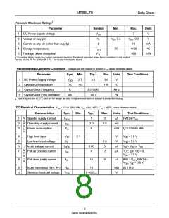
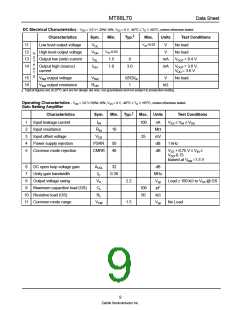
DC Electrical Characteristics - VDD = 3.0 V+ 20%/-10%, VSS = 0 V, -40°C ≤ TO ≤ +85°C, unless otherwise stated.
Characteristics
Sym.
Min.
Typ.‡
Max.
Units
Test Conditions
No load
VSS+0.03
11
12
13
14
Low level output voltage
High level output voltage
Output low (sink) current
VOL
VOH
IOL
V
V
VDD-0.03
1.5
No load
O
U
T
8
mA
mA
VOUT = 0.4 V
P
U
T
Output high (source)
current
IOH
1.0
3.0
VOUT = 3.6 V,
DD = 3.6 V
V
S
15
16
VRef output voltage
VRef
ROR
0.512VDD
1
V
No load
VRef output resistance
kΩ
‡ Typical figures are at 25°C and are for design aid only: not guaranteed and not subject to production testing.
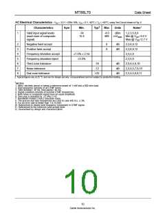
Operating Characteristics - VDD = 3.0 V+20%/-10%, VSS = 0 V, -40°C ≤ TO ≤ +85°C, unless otherwise stated.
Gain Setting Amplifier
Characteristics
Sym.
Min. Typ.‡ Max. Units
Test Conditions
VSS ≤ VIN ≤ VDD
1
2
3
4
5
Input leakage current
Input resistance
IIN
RIN
100
nA
MΩ
mV
dB
10
Input offset voltage
Power supply rejection
Common mode rejection
VOS
25
PSRR
CMRR
50
40
1 kHz
VSS + 0.75 V ≤ VIN
dB
≤
V
DD-0.75
biased at VRef =1.5 V
Load ≥ 100 kΩ to VSS @ GS
No Load
6
7
8
9
DC open loop voltage gain
Unity gain bandwidth
AVOL
fC
32
dB
MHz
Vpp
pF
0.30
Output voltage swing
VO
2.2
1.5
Maximum capacitive load (GS)
CL
100
50
10 Resistive load (GS)
11 Common mode range
RL
kΩ
VCM
Vpp
9
Zarlink Semiconductor Inc.

 ZARLINK [ ZARLINK SEMICONDUCTOR INC ]