MT88E46 Advance Information
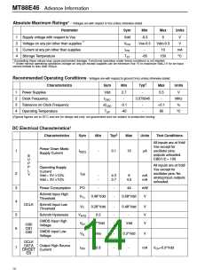
Absolute Maximum Ratings* - Voltages are with respect to Vss unless otherwise stated
Parameter
Sym
Min
Max
Units
1
2
3
4
Supply voltage with respect to Vss
Voltage on any pin other than supplies
Current at any pin other than supplies
Storage Temperature
Vdd
VPIN
IPIN
-0.3
Vss-0.3
-
6
Vdd+0.3
10
V
V
**
mA
oC
TST
-65
150
* Exceeding these values may cause permanent damage. Functional operation under these conditions is not implied.
** Under normal operating conditions voltage on any pin except supplies can be minimum Vss-1V to maximum Vdd+1V for an input
current limited to less than 200µA.
Recommended Operating Conditions - Voltages are with respect to ground (Vss) unless otherwise stated
‡
Characteristics
Sym
Min
Typ
Max
Units
1
2
3
4
Power Supplies
Clock Frequency
Vdd
fOSC
∆fOSC
TOP
2.7
-
-
5.5
-
V
MHz
%
3.579545
Tolerance on Clock Frequency
Operating Temperature
-0.1
-40
-
-
+0.1
85
oC
‡Typical figures are at 25˚C and are for design aid only: not guaranteed and not subject to production testing.
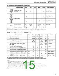
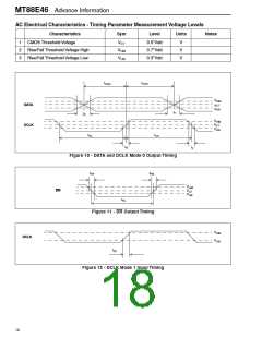
DC Electrical Characteristics†
‡
Characteristics
Sym
Min
Typ
Max
Units
Test Conditions
All inputs are at Vdd/
Vss except for
oscillator pins,
outputs unloaded.
CB0/1/2 = 100
Power Down Mode
Supply Current
1
2
I
-
0.1
15
µA
DDQ
S
U
P
P
L
All inputs are at Vdd/
Vss except for
oscillator pins. No
analog input, outputs
unloaded.
Operating Supply
Current
Vdd = 5V 10%
Vdd = 3V 10%
I
DD
Y
-
-
4.3
2.7
8
4.5
mA
mA
3
4
5
6
Power Consumption
PO
-
-
-
44
mW
V
Schmitt Input High
Threshold
V
0.48*Vdd
0.68*Vdd
T+
DCLK
Schmitt Input Low
Threshold
V
0.28*Vdd
0.2
-
-
-
0.48*Vdd
V
V
V
T-
Schmitt Hysteresis
V
-
HYS
CMOS Input High
Voltage
V
0.7*Vdd
Vdd
IH
CB0
CB1
CB2
CMOS Input Low
Voltage
V
Vss
0.8
-
-
0.3*Vdd
-
V
IL
DCLK
DATA
DR/DET
CD
Output High Source
Current
7
I
mA
VOH=0.9*Vdd
OH
14

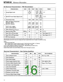
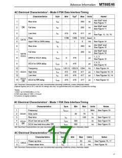
 ZARLINK [ ZARLINK SEMICONDUCTOR INC ]