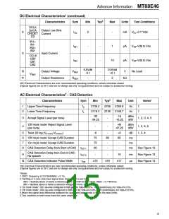
Advance Information MT88E46
down. The two input op-amps are not affected and
both will remain operational.
Maximum Drive Level:
e.g. CTS MP036S
2mW
The partial power down feature can also be used to
reset the FSK or CAS circuits, such as upon system
power up. To reset the FSK demodulator, use CB1/2
to select CAS mode for about 10µs, DR will become
high. To reset the CAS detector, select FSK mode for
about 10µs, DET will become high.
Alternatively an external clock source can be used.
In which case the OSC1 pin should be driven directly
from a CMOS buffer and the OSC2 pin left open.
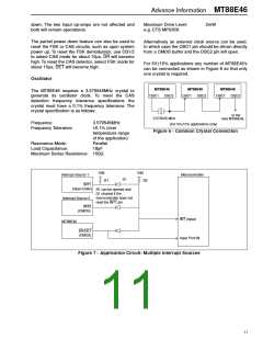
For 5V 10% applications any number of MT88E46’s
can be connected as shown in Figure 6 so that only
one crystal is required.
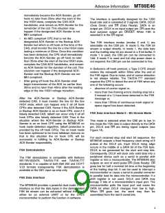
Oscillator
MT88E46
OSC1 OSC2
MT88E46
OSC1 OSC2
MT88E46
OSC1 OSC2
The MT88E46 requires a 3.579545MHz crystal to
generate its oscillator clock. To meet the CAS
detection frequency tolerance specifications the
crystal must have a 0.1% frequency tolerance. The
crystal specification is as follows:
to the
next MT88E46
3.579545 MHz
(For 5V 10% applications only)
Frequency:
Frequency Tolerance:
3.579545MHz
0.1% (over
Figure 6 - Common Crystal Connection
temperature range
of the application)
Parallel
Resonance Mode:
Load Capacitance:
18pF
Maximum Series Resistance: 150Ω
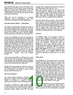
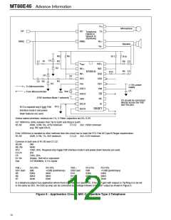
Vdd
Vdd
R2
Microcontroller
Interrupt Source 1
D1
R1
INT1
(Open Drain)
R1 can be opened and
D1 shorted if the
microcontroller does not
read the INT1 pin.
Interrupt Source 2
INT2
(CMOS)
INT (input)
MT88E46
DR/DET
(CMOS)
Input Port Bit
Figure 7 - Application Circuit: Multiple Interrupt Sources
11

 ZARLINK [ ZARLINK SEMICONDUCTOR INC ]