MT88E46 Advance Information
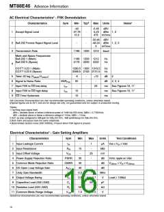
AC Electrical Characteristics† - FSK Demodulation
‡
Characteristics
Sym
Min
Typ
Max
Units
Notes*
-40
-37.78
10.0
-6.45
-4.23
476 mVrms
dBV
dBm 1, 2
1 Accept Signal Level
-
-50.46 dBV
2 Bell 202 Format Reject Signal Level
3 Transmission Rate
-
-
-48.24 dBm 1, 2, 3
3
mVrms
1188 1200 1212
baud
Mark and Space Frequencies
Bell 202 1 (Mark)
Bell 202 0 (Space)
1188 1200 1212
2178 2200 2222
Hz
Hz
4
CCITT V.23 1 (Mark)
CCITT V.23 0 (Space)
1280.5 1300 1319.5
2068.5 2100 2131.5
Hz
Hz
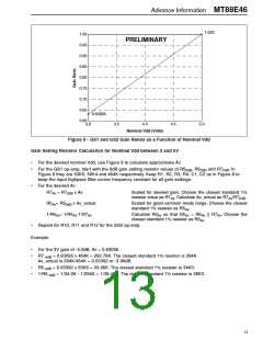
5 Twist: 20 log (VMARK/VSPACE
)
-6
20
-
-
-
-
-
-
+10
dB
dB
2
6 Signal to Noise Ratio
SNRFSK
tCP
-
25
-
2, 3, 4
7 Input FSK to CD low delay
8 Input FSK to CD high delay
9 CD Time Hysteresis
ms See Figures 16, 17
ms See Figures 16, 17
ms
tCA
10
10
-
†AC Electrical Characteristics are over recommended operating conditions, unless otherwise stated.
‡Typical figures are at 25˚C and are for design aid only: not guaranteed and not subject to production testing.
*Notes:
1.Tip/Ring input signal level.
dBm = decibels above or below a reference power of 1mW into 600 ohms. 0dBm = 0.7746Vrms.
dBV = decibels above or below a reference voltage of 1Vrms. 0dBV = 1Vrms.
2.GS1 op-amp configured to 0dB gain for Vdd=5V 10%, -4dB (preliminary) for Vdd=3V 10%.
3.Both mark and space have the same amplitude.
4.Band limited random noise (300-3400Hz). Present when FSK signal is present.
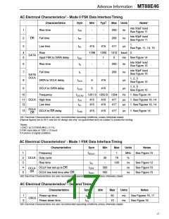
Electrical Characteristics† - Gain Setting Amplifiers
Characteristics
Input Leakage Current
Sym
Min
Max
Units
Test Conditions
Vss ≤ VIN ≤ Vdd
1
2
3
4
5
6
7
8
9
IIN
RIN
-
10
-
1
µA
MΩ
mV
dB
dB
dB
MHz
V
Input Resistance
-
Input Offset Voltage
VOS
PSRR
CMRR
AVOL
fC
25
Power Supply Rejection Ratio
Common Mode Rejection Ratio
DC Open Loop Voltage Gain
Unity Gain Bandwidth
30
40
40
0.3
0.5
-
-
1kHz ripple on Vdd
-
VCMmin ≤ VIN ≤ VCMmax
-
-
Vdd-0.7
50
Output Voltage Swing
VO
Load ≥ 100kΩ
Capacitive Load (GS1,GS2)
CL
pF
10 Resistive Load (GS1,GS2)
RL
100
1.0
-
kΩ
V
11 Common Mode Range Voltage
VCM
Vdd-1.0
†Electrical characteristics are over recommended operating conditions, unless otherwise stated.
16

 ZARLINK [ ZARLINK SEMICONDUCTOR INC ]