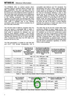
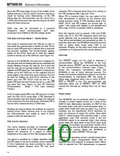
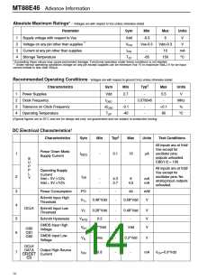
MT88E46 Advance Information
Since the DR rising edge occurs in the middle of the
trailing stop bit, it can be used to read the stop bit to
check for framing error. Alternatively, at the DR
falling edge the microcontroller can set a timer for a
1/2400 second timeout and read the stop bit at DATA
when the timer times out.
activated. CD is released when there is no activity at
the FSK bandpass filter output for 10ms.
When CD is inactive (high), the raw output of the
FSK demodulator is ignored by the internal data
timing recovery circuit. In FSK interface mode 0 the
DATA, DCLK and DR outputs are forced high. In
mode 1 the output shift register is not updated and
DR is high; if DCLK is clocked, DATA is undefined.
DATA may also be connected to a personal
computer’s serial communication port after
conversion from CMOS to RS-232 voltage levels.
Note that signals such as speech, CAS and DTMF
tones also lie in the FSK frequency band and the
carrier detector may be activated by these signals.
They will be demodulated and presented as data. To
avoid the false data, the MT88E46 should be put into
CAS or power down mode when FSK is not
expected. Ringing, on the other hand, does not pose
a problem as it is ignored by the carrier detector.
FSK Data Interface Mode 1 - Buffer Mode
This mode is selected when the CB0 pin is high. In
this mode the received byte is stored on chip. At the
end of a byte DR goes low to indicate that a new byte
has become available. The microcontroller applies
pulses at the DCLK input pin to read the register
contents serially out of the DATA pin (see Figure 15).
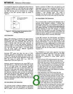
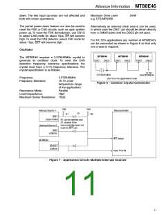
Interrupt
The DR/DET output can be used to interrupt a
microcontroller. When the MT88E46 is the only
interrupt source, DR/DET can be connected directly
to the microcontroller’s interrupt input. Figure 7
shows the necessary connections when the
MT88E46 is one of many interrupt sources. The
diodes and resistors implement a wired-or so that the
microcontroller is interrupted (INT low active or
falling edge triggered) when one or more of INT1,
INT2 or DR/DET is low. The microcontroller can
determine which one of DR/DET, INT1 or INT2
caused the interrupt by reading them into an input
port.
Internal to the MT88E46, the start bit is stripped off,
the data bits and the trailing stop bit are sampled and
stored. Midway through the stop bit, the 8 data bits
and the stop bit are parallel loaded into a 9 bit shift
register and DR goes low. The register’s contents are
shifted out to the DATA pin on the supplied DCLK’s
rising edges in the order they were received. The last
bit must be shifted out and DCLK returned to low
before the next DR. DCLK must be low for tDDS
before DR goes low and remain low for tDDH after DR
has gone low (see Figure 15 and ‘AC Electrical
Characteristics - Mode 1 FSK Data Interface
Timing’).
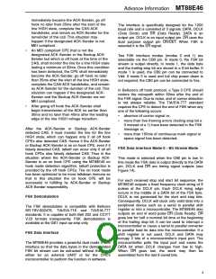
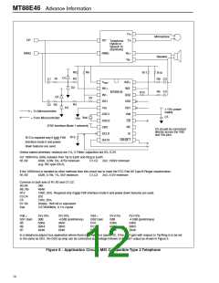
Power Down
If DCLK begins while DR is low, DR will return to high
upon the first DCLK rising edge. If DR interrupts a
microcontroller then this feature allows the interrupt
to be cleared by the first read pulse. Otherwise DR is
low for half a nominal bit time (1/2400 sec).
The MT88E46 can be powered down to consume
virtually no power supply current via a state of the
CB0/1/2 pins. Momentary transition of CB0/1/2 into
the power down code will not activate power down. In
power down mode both input op-amps, VREF and the
oscillator are not operational; DCLK becomes an
input pin because to select the power down state
CB0 is 1 which selects FSK interface mode 1. If the
application uses FSK interface mode 0 and the
MT88E46 needs to be powered down, then during
power down the input state of the DCLK input must
be defined, for example, by a pull down resistor (R13
in Figure 8) so that the MT88E46 will draw minimal
power supply current. When the MT88E46 is
powered down DATA, DR/DET, CD are high.
Reading the stop bit allows the software to check for
framing errors. When framing error is not checked
the microcontroller only needs to send 8 DCLK
pulses to shift the data byte out.
FSK Carrier Detector
The carrier detector provides an indication of the
presence of a signal in the FSK frequency band. It
detects the presence of a signal of sufficient
amplitude at the output of the FSK bandpass filter.
To reduce the operating current a partial power down
feature has been incorporated. When FSK is
selected, the CAS detector is powered down. When
CAS is selected the FSK demodulator is powered
The signal is qualified by a digital algorithm before
the CD output is set low to indicate carrier detection.
A 10ms hysteresis has been provided to allow for
momentary signal dropout once CD has been
10

 ZARLINK [ ZARLINK SEMICONDUCTOR INC ]