MT3170B/71B, MT3270B/71B, MT3370B/71B
Data Sheet
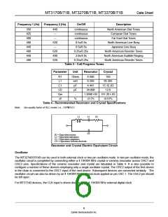
Frequency 1 (Hz)
Frequency 2 (Hz)
On/Off
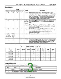
Description
350
425
400
480
440
480
440
480
440
---
---
620
---
620
480
620
continuous
continuous
continuous
0.5s/0.5s
0.5s/0.5s
0.25s/0.25s
2.0s/4.0s
North American Dial Tones
European Dial Tones
Far East Dial Tones
North American Line Busy
Japanese Line Busy
North American Reorder Tones
North American Audible Ringing
North American Reorder Tones
0.25s/0.25s
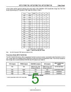
Table 3 - Call Progress Tones
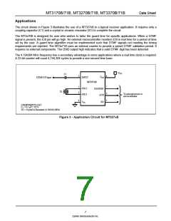
Parameter
Unit
Resonator
Crystal
R1
L1
C1
C0
Qm
∆f
Ohms
mH
pF
pF
-
6.580
0.359
4.441
34.890
1.299E+03 101.2E+ 03
±0.2% ±0.01%
150
95.355
15.1E-03
12.0
%
Table 4 - Recommended Resonator and Crystal Specifications
Note:
Qm=quality factor of RLC model, i.e., 1/2P¶R1C1.
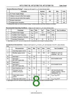
L1
C1
C0
R1
R1 = Equivalent resistor.
L1 = Equivalent inductance.
C1 = Equivalent compliance.
C0 = Capacitance between electrode.
Resonator and Crystal Electric Equivalent Circuit
Oscillator
The MT327xB/337xB can be used in both external clock or two pin oscillator mode. In two pin oscillator mode, the
oscillator circuit is completed by connecting either a 4.194304 MHz crystal or ceramic resonator across OSC1 and
OSC2 pins. Specifications of the ceramic resonator and crystal are tabulated in Table 4. It is also possible to
configure a number of these devices employing only a single oscillator crystal. The OSC2 output of the first device
in the chain is connected to the OSC1 input of the next device. Subsequent devices are connected similarly. The
oscillator circuit can also be driven by an 4.194304 MHz external clock applied on pin OSC 1. The OSC2 pin should
be left open.
For MT317xB devices, the CLK input is driven directly by an 4.194304 MHz external digital clock.
6
Zarlink Semiconductor Inc.

 ZARLINK [ ZARLINK SEMICONDUCTOR INC ]