MT3170B/71B, MT3270B/71B, MT3370B/71B
Data Sheet
Description
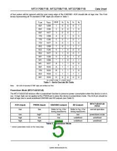
The MT3x7xB is a family of high performance DTMF receivers which decode all 16 tone pairs into a 4-bit binary
code. These devices incorporate an AGC for wide dynamic range and are suitable for end-to-end signalling. The
MT3x70B provides an early steering (ESt) logic output to indicate the detection of a DTMF signal and requires
external software guard time to validate the DTMF digit. The MT3x71B, with preset internal guard times, uses a
delay steering (DStD) logic output to indicate the detection of a valid DTMF digit. The 4-bit DTMF binary digit can be
clocked out synchronously at the serial data (SD) output. The SD pin is multiplexed with call progress detector
output. In the presence of supervisory tones, the call progress detector circuit indicates the cadence (i.e., envelope)
of the tone burst. The cadence information can then be processed by an external microcontroller to identify specific
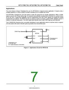
call progress signals. The MT327xB and MT337xB can be used with a crystal or a ceramic resonator without
additional components. A power-down option is provided for the MT317xB and MT337xB.
MT3370BN/71BN
MT3170B/71B
MT3270B/71B
MT3370BS/71BS
20
19
18
17
16
15
14
13
12
11
1
2
NC
NC
NC
18
17
16
15
14
13
12
11
10
1
2
3
4
5
6
7
8
9
NC
INPUT
PWDN
OSC2
NC
VDD
NC
NC
INPUT
PWDN
CLK
VDD INPUT
VDD
1
2
3
4
8
7
6
5
1
2
3
4
8
7
6
5
INPUT
PWDN
NC
3
4
5
VDD
NC
NC
ESt/
ESt/
OSC2
DStD
ESt/DStD
NC
ESt/DStD
NC
DStD
6
7
OSC2
OSC1
VSS
OSC1
ACK
ACK
OSC1
NC
ACK
NC
ACK
SD
8
VSS
VSS
SD
SD
NC
SD
9
NC
NC
VSS
NC
NC
10
NC
8 PIN PLASTIC DIP
18 PIN PLASTIC SOIC
20 PIN SSOP
Figure 2 - Pin Connections
Name
Pin Description
Pin #
Description
337xBN 337xBS 327xB
317xB
3
2
1
1
INPUT DTMF/CP Input. Input signal must be AC coupled via
capacitor.
6
7
4
6
2
3
-
3
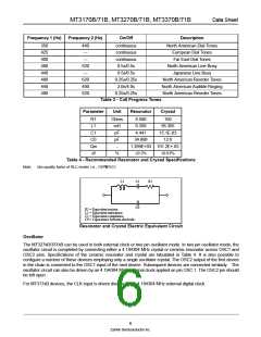
OSC2 Oscillator Output.
OSC1 Oscillator/Clock Input. This pin can either be driven by:
(CLK) 1) an external digital clock with defined input logic levels.
OSC2 should be left open.
2) connecting a crystal or ceramic resonator between
OSC1 and OSC2 pins.
8
13
9
11
4
5
4
5
VSS
SD
Ground. (0V)
Serial Data/Call Progress Output. This pin serves the dual
function of being the serial data output when clock pulses are
applied after validation of DTMF signal, and also indicates
the cadence of call progress input. As DTMF signal lies in
the same frequency band as call progress signal, this pin
may toggle for DTMF input. The SD pin is at logic low in
powerdown state.
2
Zarlink Semiconductor Inc.

 ZARLINK [ ZARLINK SEMICONDUCTOR INC ]