MT3170B/71B, MT3270B/71B, MT3370B/71B
Data Sheet
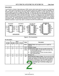
Pin Description
Pin #
Name
Description
337xBN 337xBS 327xB
317xB
14
13
6
6
ACK
Acknowledge Pulse Input. After ESt or DStD is high,
applying a sequence of four pulses on this pin will then shift
out four bits on the SD pin, representing the decoded DTMF
digit. The rising edge of the first clock is used to latch the 4-
bit data prior to shifting. This pin is pulled down internally.
The idle state of the ACK signal should be low.
16
15
7
7
ESt
Early Steering Output. A logic high on ESt indicates that a
DTMF signal is present. ESt is at logic low in powerdown
state.
(MT3x70B)
DStD
Delayed Steering Output. A logic high on DStD indicates
that a valid DTMF digit has been detected. DStD is at logic
low in powerdown state.
(MT3x71B)
18
18
8
-
8
-
VDD
NC
Positive Power Supply (5 V Typ.) Performance of the
device can be optimized by minimizing noise on the supply
rails. Decoupling capacitors across VDD and VSS are
therefore recommended.
1,2,5,9,
1,5,7,8,
No Connection. Pin is unconnected internally.
10,11,12, 10, 12,
15,17,19,20 14,16,
17
4
3
-
2
PWDN Power Down Input. A logic high on this pin will power down
the device to reduce power consumption. This pin is pulled
down internally and can be left open if not used. ACK pin
should be at logic ’0’ to power down device.
Summary of MT3x70/71B Product Family
2 Pin
Device
Type
Ext
8 Pin
18 Pin
20 Pin
PWDN
ESt
DStD
OSC
CLK
MT3170B
MT3171B
MT3270B
MT3271B
MT3370B
MT3371B
√
√
√
√
√
√
√
√
√
√
√
√
√
√
√
√
√
√
√
√
√
√
√
√
√
√
√
√
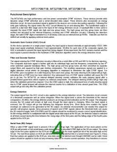
Change Summary
The following table summarizes the changes from the August 2006 issue.
Page
Item
Figure 2
“Pin Description“
Description
2
2
Added ordering codes to Pin Connection diagram.
Added 20 pin description to the table.
3
Zarlink Semiconductor Inc.

 ZARLINK [ ZARLINK SEMICONDUCTOR INC ]