MT3170B/71B, MT3270B/71B, MT3370B/71B
Data Sheet
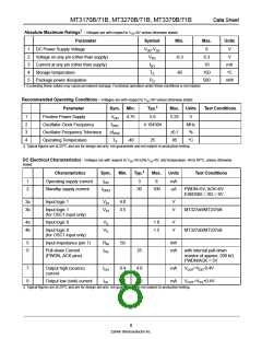
Absolute Maximum Ratings† - Voltages are with respect to VSS=0V unless otherwise stated.
Parameter
DC Power Supply Voltage
Symbol
Min.
Max.
Units
1
2
3
4
5
V
DD-VSS
VI/O
II/O
6
V
V
Voltage on any pin (other than supply)
Current at any pin (other than supply)
Storage temperature
-0.3
-65
6.3
10
mA
°C
TS
150
500
Package power dissipation
† Exceeding these values may cause permanent damage. Functional operation under these conditions is not implied.
PD
mW
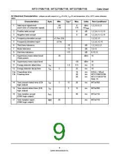
Recommended Operating Conditions - Voltages are with respect to VSS=0V unless otherwise stated
Parameter
Sym.
Min.
Typ.‡
Max. Units
Test Conditions
1
2
3
4
Positive Power Supply
VDD
fOSC
∆fOSC
Td
4.75
5.0
5.25
V
MHz
%
Oscillator Clock Frequency
Oscillator Frequency Tolerance
Operating Temperature
4.194304
±0.1
85
-40
25
°C
‡ Typical figures are at 25°C and are for design aid only: not guaranteed and not subject to production testing.
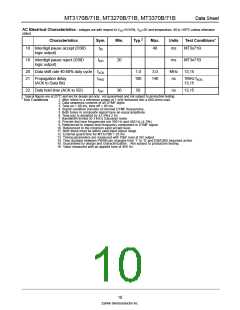
DC Electrical Characteristics - Voltages are with respect to VDD=5V±5%,VSS=0V, and temperature -40 to 85°C, unless otherwise
stated.
Characteristics
Sym.
Min.
Typ.‡
Max.
Units
Test Conditions
1
2
Operating supply current
Standby supply current
IDD
3
8
mA
IDDQ
30
100
µA
PWDN=5V, ACK=0V
ESt/DStD = SD = 0V
3a
3b
Input logic 1
VIH
VIH
4.0
3.5
V
V
Input logic 1
MT327xB/MT337xB
MT327xB/MT337xB
(for OSC1 input only)
4a
4b
Input logic 0
VIL
VIL
1.0
1.5
V
V
Input logic 0
(for OSC1 input only)
5
6
Input impedance (pin 1)
RIN
IPD
50
kW
mA
Pull-down Current
(PWDN, ACK pins)
25
with internal pull-down
resistor of approx. 200 kΩ.
PWDN/ACK = 5V
7
8
Output high (source)
current
IOH
IOL
0.4
1.0
4.0
9.0
mA
mA
VOUT=VDD-0.4V
Output low (sink) current
‡ Typical figures are at 25°C and are for design aid only: not guaranteed and not subject to production testing.
VOUT=VSS+0.4V
8
Zarlink Semiconductor Inc.

 ZARLINK [ ZARLINK SEMICONDUCTOR INC ]