MA17503
1.0 SYSTEM CONSIDERATIONS
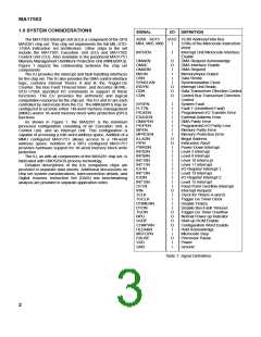
SIGNAL
I/O
DEFINITION
AD00 - AD15
M04, M05, M06
I/O/Z 16-Bit Address/Data Bus
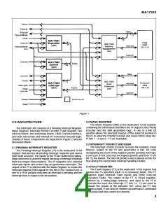
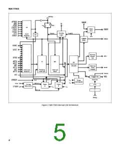
The MA17503 Interrupt Unit (IU) is a component of the GPS
MAS281 chip set. This chip set implements the full MIL-STD-
1750A instruction set architecture. Other chips in the set
include the MA17501 Execution Unit (EU) and MA17502
Control Unit (CU). Also available is the peripheral MA31751
Memory Management Unit/Block Protection Unit (MMU(BPU)).
Figure 1 depicts the relationship between the chip set
components.
The IU provides the interrupt and fault handling interfaces
for the chip set. The IU also provides the DMA control interface
logic, contains interval Timers A and B, the Trigger-Go
Counter, the Bus Fault Timeout timer, and decodes all MIL-
STD-1750A specified l/O commands in support of these
functions. The EU provides the arithmetic and logical
computation resources for the chip set. The EU and IU are each
controlled by microcode from the CU. The MMU(BPU) may be
configured to provide either 1M-word memory management
(MMU) and/or 1K-word memory block write protection (BPU)
functions.
As shown in Figure 1, the MAS281 is the minimum
processor configuration consisting of an Execution Unit, a
Control Unit, and an Interrupt Unit. This configuration is
capable of accessing a 64K-word address space. Addition of a
MMU configured MA31751 allows access to a 1M-word
address space. Addition of a BPU configured MA31751
provides hardware support for 1K-word memory block write
protection.
I
I
3 Bits of the Mlcrocode Instruction
Word
Interrupt Unit Microcode Interface
Enable
INTREN
DMAKN
DMAE
DMARN
M/ION
DSN
SYNCLKN
IRDYN
DDN
O
O
I
DMA Request Acknowledge
DMA Interface Enable
DMA Request
I
I
Memory/lnput-Output
Data Strobe
I
Synchronisation Clock
Interrupt Unit Ready
Data Transceiver Dlrection Control
Control Bus Transceiver Direction
Control
O
O
O
CDN
SYSFN
FLT7N
PIOXEN
EXADEN
DMAPEN
PIOPEN
MPEN
MPROEN
ILLADN
PIFN
PWRDN
INT02N
INT08N
INT10N
INT11N
IOI1N
INT13N
IOI2N
INT15N
OV1N
IRN
TCLK
TGCLK
DTIMERN
DTON
TGON
NPlJ
I
I
I
I
I
System Fault
Fault 7 (Undefined Fault)
Programmed I/O Transfer Error
External Address Error
DMA Parity Error
I
I
I
O
O
I
Programmed I/O Parity Lrror
Memory Parity Error
Memory Protection Error
Illegal Address
Instruction Abort
Power-Down Interrupt
Level 2 Interrupt
I
I
Level 8 Interrupt
The IU, as with all components of the MAS281 chip set, is
fabricated with CMOS/SOS process technology.
I
Level 10 Interru pt
I
Level 11 Interrupt
Detailed descriptions of the lUs companion chips are
provided in separate data sheets. Additional discussions on
chip set system considerations, interconnection details, and
Digital Avionics Instruction Set (DAIS) mix benchmarking
analysis are provided in separate application notes.
I
I
I/O Register Interrupt 1
Level 13 Interrupt
I
I
I/O Register Interrupt 2
Level 15 Interrupt
I
O
I
I
I
Fixed-Point Overflow Interrupt
Interrupt Request
Clock for Tlmers A and B
Trigger Go Timer Clock
Disable Timers
I
Disable Bus-Fault Timeout
Trigger-Go Timer Overflow
Normal Power-up Indicator
Start-up ROM Enable
Configuration Word Enable
Hold Acknowledge
Microcode Stop
O
O
O
O
I
SURE
CONFWN
HLDAKN
MSTOPN
PAUSE
VDD
I
O
I
Processor Pause
Power
GND
I
Ground
Table 1: Signal Definitions
2

 ZARLINK [ ZARLINK SEMICONDUCTOR INC ]