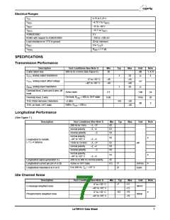
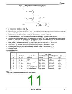
Figure 1. AC Input Impedance Programming Network
VTX
RT1 = 150 k
Ω
Ω
CT1 = 60 pF
RT2 = 150 k
RSN
RRX = 300 k
Ω
VRX
2. a. Overload level is defined when THD = 1%.
b. Overload level is defined when THD = 1.5%.
3. Balance return signal is the signal generated at V by V . This specification assumes that the two-wire AC load impedance matches the
TX
RX
programmed impedance.
4. Not tested in production. This parameter is guaranteed by characterization or correlation to other tests.
5. This parameter is tested at 1 kHz in production. Performance at other frequencies is guaranteed by characterization.
6. Group delay can be greatly reduced by using a Z network such as that shown in Note 1 above. The network reduces the group delay to
T
less than 2 µs and increases Two-Wire Return Loss. The effect of group delay on linecard performance may also be compensated for by
synthesizing complex impedance with the QSLAC or DSLAC device.
7. 90 Vpk provides 57 Vrms with a crest factor of 1.4 to a load of 1400 Ω with 2 • R = 100, and R
= 70 Ω (1570 Ω).
LINE
F
8. Open Circuit V can be modified using RSGH. Longitudinal voltage in OHT state is 30 V limiting V to 60 V.
AB
AB
9.
R
must be greater than 52 kΩ. See “User-Programmable Components” on page 12 for typical value of R
.
LTH
D
10. Conforms to UL1950.
SLIC DECODING
(DET) Output
State
0
1
2
3
4
5
6*
7*
C3 C2 C1
Two-Wire Status
Open Circuit
Ringing
Active
On-hook TX (OHT)
Reserved
Standby
Active Polarity Reversal
OHT Polarity Reversal
E1 = 1
Ring trip
Ring trip
Loop detector
Loop detector
Loop detector
Loop detector
Loop detector
Loop detector
E1 = 0
Ring trip
Ring trip
Ground key
Ground key
Ground key
Ground key
Ground key
Ground key
Battery
VBAT2
0
0
0
0
1
1
1
1
0
0
1
1
0
0
1
1
0
1
0
1
0
1
0
1
VBAT1
VBAT2
VBAT1
VBAT1
VBAT1
VBAT2
VBAT1
Note:
* Only –1 and –2 performance grade devices support polarity reversal.
Le79R101 Data Sheet
11

 ZARLINK [ ZARLINK SEMICONDUCTOR INC ]