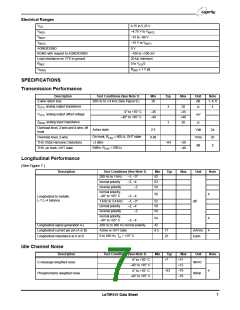
Ring Signal
Description
, Ringing
Test Conditions (See Note 1)
Ringload = 1570 Ω
Min
90
Typ
93
0
Max
Unit
Vpk
V
Note
7
V
AB
V
, Ringing offset
V
= 2.5 V
RINGIN
−5
5
AB
∆VAB ⁄ ∆VRINGIN (VRINGIN gain)
R = Open circuit
95
100
105
V/V
L
Ring input impedance to R
10 k
3
Ω
%
REF
VRING = 0.65 Vrms, R = 1570 Ω
Harmonic distortion
5
L
R = 300 Ω
Off-hook current limit
Ringing source impedance
73
83
100
93
mA
Ω
4
4
L
Ground-Key Detector Thresholds
Description
Test Conditions (See Note 1)
Min
Typ
Max
Unit
Note
Ground-key current threshold
B to ground
11
mA
Loop Detector
Description
Test Conditions (See Note 1)
Active
OHT
Min
−20
−20
−12
Typ
Max
20
20
Unit
Note
R
, Loop-resistance detect
LTH
threshold
%
9
I
, Loop-current detect threshold
Standby
12
LTH
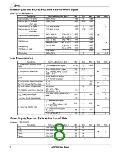
Relay Driver Output
(Relay 1 and 2)
Description
, On voltage (each output)
Test Conditions (See Note 1)
Min
Typ
+0.25
+0.30
Max
+0.4
+0.8
100
Unit
V
Note
V
V
I
I
I
= 30 mA
= 40 mA
= +5 V
OL
OL
, On voltage (each output)
4
OL
OL
, Off leakage (each output)
V
OH
µA
V
OH
I = 100 µA
Zener breakover (each output)
Zener on voltage (each output)
6.6
7.9
11
Z
I = 30 mA
Z
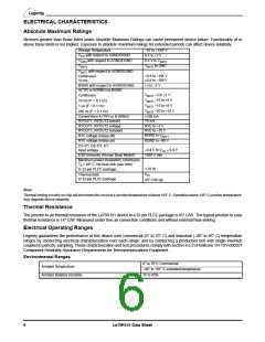
Note:
* Performance Grade
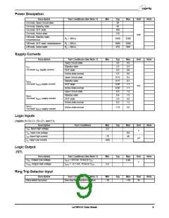
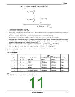
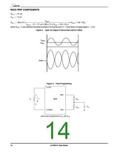
RELAY DRIVER SCHEMATIC
RYOUT1
RYOUT2
RYE
BGND
BGND
Note:
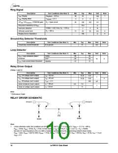
1. Unless otherwise noted, test conditions are BAT1 = –99 V, BAT2 = –21 V, V = +5 V, V
= –5 V, R = 600 Ω,
L
CC
NEG
R
= 50 kΩ, R
= 50 kΩ, R = 75 kΩ, no fuse resistors, C = 0.018 µF, C = 1.2 µF, D = D = 1N400x,
DC1
DC2 D HP DC 1 2
two-wire AC input impedance (ZSL) is a 600 Ω resistance synthesized by the programming network shown below.
R
V
= open, R
= 0 V.
= short to GND, R
= 15 kΩ, R
= 15 kΩ, C
= 10 nF, R
= 833 kΩ, R
= 42 kΩ, C = 1.0 µF,
RT2 RT
SGL
REF
SGH
DCR1
DCR2
DCR
RT1
10
Le79R101 Data Sheet

 ZARLINK [ ZARLINK SEMICONDUCTOR INC ]