R
QPRO XQ4000E/EX QML High-Reliability FPGAs
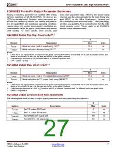
XQ4028EX Pin-to-Pin Input Parameter Guidelines
Testing of switching parameters is modeled after testing
methods specified by MIL-M-38510/605. All devices are
100% functionally tested. Pin-to-pin timing parameters are
derived from measuring external and internal test patterns
and are guaranteed over worst-case operating conditions
(supply voltage and junction temperature). Listed below are
representative values for typical pin locations and normal
clock loading. For more specific, more precise, and
worst-case guaranteed data, reflecting the actual routing
structure, use the values provided by the static timing ana-
lyzer (TRCE in the Xilinx Development System) and
back-annotated to the simulation netlist. These path delays,
provided as a guideline, have been extracted from the static
timing analyzer report. Values apply to all XQ4000EX
devices unless otherwise noted
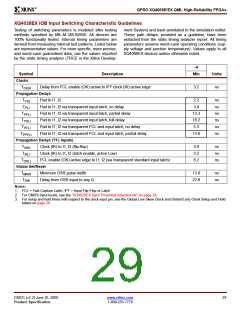
XQ4028EX Global Low Skew Clock, Setup and Hold
-4
Min
8.0
0
Symbol
Description
Units
ns
T
Input setup time, using Global Low Skew clock and IFF (full delay)
Input hold time, using Global Low Skew clock and IFF (full delay)
PSD
PHD
T
ns
Notes:
1. IFF = Flip-Flop or Latch
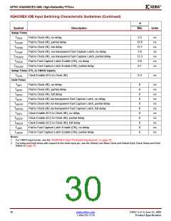
XQ4028EX Global Early Clock, Setup and Hold for IFF
-4
(2)
Symbol
Description
Min
Units
ns
T
Input setup time, using Global Early clock and IFF (full delay)
Input hold time, using Global Early clock and IFF (full delay)
6.5
0
PSEP
PHEP
T
ns
Notes:
1. IFF = Flip-Flop or Latch
2. Setup parameters are for BUFGE #s 3, 4, 7 and 8. Add 1.6 ns for BUFGE #s 1, 2, 5 and 6.
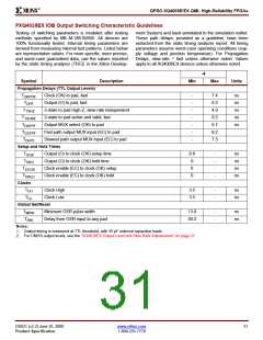
XQ4028EX Global Early Clock, Setup and Hold for FCL
-4
(2)
Symbol
Description
Min
3.4
0
Units
ns
T
Input setup time, using Global Early clock and FCL (partial delay)
Input hold time, using Global Early clock and FCL (partial delay)
PFSEP
PFHEP
T
ns
Notes:
1. FCL = Fast Capture Latch
2. For CMOS input levels, see the XQ4028EX Input Threshold Adjustments.
3. Setup time is measured with the fastest route and the lightest load. Use the static timing analyzer to determine the setup time under
given design conditions.
4. Hold time is measured using the farthest distance and a reference load of one clock pin per two IOBs. Use the static timing analyzer
to determine the setup and hold times under given design conditions.
5. Setup parameters are for BUFGE #s 3, 4, 7 and 8. Add 1.2 ns for BUFGE #s 1, 2, 5 and 6.
XQ4028EX Input Threshold Adjustments
The following table must be used to adjust input parameters and input switching characteristics.
-4
Symbol
Description
Max
0
Units
ns
T
For TTL input add
TTLI
T
For CMOS input add
0.3
ns
CMOSI
28
www.xilinx.com
DS021 (v2.2) June 25, 2000
1-800-255-7778
Product Specification

 XILINX [ XILINX, INC ]