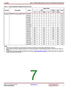
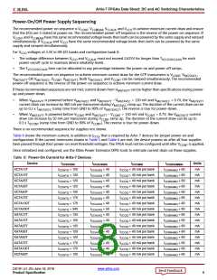
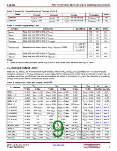
Artix-7 FPGAs Data Sheet: DC and AC Switching Characteristics
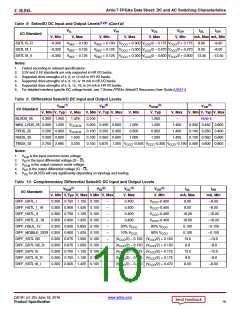
Table 10: Complementary Differential SelectIO DC Input and Output Levels (Cont’d)
(1)
(2)
(3)
(4)
VICM
V, Min V,Typ V, Max V,Min V, Max
0.300 0.900 1.425 0.100
VID
VOL
V, Max
(VCCO/2) – 0.600 (VCCO/2) + 0.600
VOH
IOL
mA, Max
13.4
IOH
I/O Standard
V, Min
mA, Min
–13.4
DIFF_SSTL18_II
–
Notes:
1.
2.
3.
4.
V
V
V
V
is the input common mode voltage.
is the input differential voltage (Q – Q).
is the single-ended low-output voltage.
ICM
ID
OL
OH
is the single-ended high-output voltage.
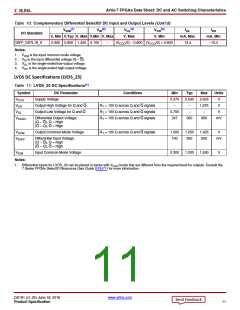
LVDS DC Specifications (LVDS_25)
(1)
Table 11: LVDS_25 DC Specifications
Symbol
VCCO
VOH
DC Parameter
Supply Voltage
Conditions
Min
Typ
2.500
–
Max
Units
2.375
–
2.625
1.675
–
V
V
Output High Voltage for Q and Q
Output Low Voltage for Q and Q
RT = 100 Ω across Q and Q signals
RT = 100 Ω across Q and Q signals
RT = 100 Ω across Q and Q signals
VOL
0.700
247
–
V
VODIFF
Differential Output Voltage:
(Q – Q), Q = High
350
600
mV
(Q – Q), Q = High
VOCM
VIDIFF
Output Common-Mode Voltage
RT = 100 Ω across Q and Q signals
1.000
100
1.250
350
1.425
600
V
Differential Input Voltage:
(Q – Q), Q = High
mV
(Q – Q), Q = High
VICM
Input Common-Mode Voltage
0.300
1.200
1.500
V
Notes:
1. Differential inputs for LVDS_25 can be placed in banks with V
levels that are different from the required level for outputs. Consult the
CCO
7 Series FPGAs SelectIO Resources User Guide (UG471) for more information.
DS181 (v1.25) June 18, 2018
www.xilinx.com
Product Specification
11

 XILINX [ XILINX, INC ]