Artix-7 FPGAs Data Sheet: DC and AC Switching Characteristics
A similar part naming convention applies to the speed specifications selection in the ISE tools for supported devices. See
Table 14 for the subset of 7 series FPGAs supported in the ISE tools.
Performance Characteristics
This section provides the performance characteristics of some common functions and designs implemented in Artix-7
devices. The numbers reported here are worst-case values; they have all been fully characterized. These values are subject to
the same guidelines as the AC Switching Characteristics, page 12.
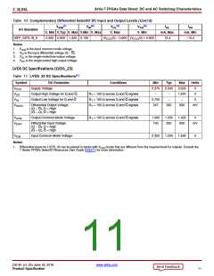
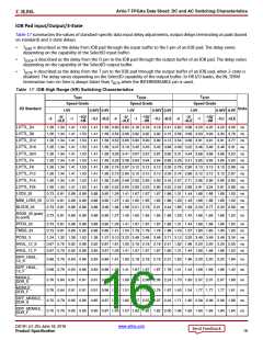
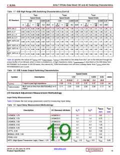
Table 15: Networking Applications Interface Performances
Speed Grade
Description
1.0V
-2/-2LE
680
0.95V
-1LI
600
0.9V
-2LE
600
Units
-3
-1
SDR LVDS transmitter (using OSERDES; DATA_WIDTH = 4 to 8)
DDR LVDS transmitter (using OSERDES; DATA_WIDTH = 4 to 14)
SDR LVDS receiver (SFI-4.1)(1)
680
600
950
600
950
Mb/s
Mb/s
Mb/s
Mb/s
1250
680
1250
680
950
950
600
600
DDR LVDS receiver (SPI-4.2)(1)
1250
1250
950
950
Notes:
1. LVDS receivers are typically bounded with certain applications where specific dynamic phase-alignment (DPA) algorithms dominate
deterministic performance.
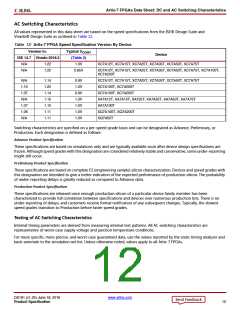
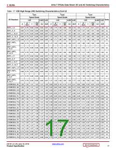
Table 16: Maximum Physical Interface (PHY) Rate for Memory Interfaces IP available with the Memory Interface
(1)(2)
Generator
Speed Grade
Memory Standard
1.0V
0.95V
-1LI
0.9V
-2LE
Units
-3
-2/-2LE
-1
-1Q/-1M
4:1 Memory Controllers
DDR3
1066(3)
800
800
800
800
800
667
667
667
N/A
533
800
667
667
800
667
667
Mb/s
Mb/s
Mb/s
DDR3L
DDR2
800
2:1 Memory Controllers
DDR3
800
800
800
667
700
700
700
667
620
620
620
533
620
N/A
533
400
620
620
620
533
620
620
620
533
Mb/s
Mb/s
Mb/s
Mb/s
DDR3L
DDR2
LPDDR2
Notes:
1.
V
tracking is required. For more information, see 7 Series FPGAs Memory Interface Solutions User Guide (UG586).
REF
2. When using the internal V
, the maximum data rate is 800 Mb/s (400 MHz).
REF
3. The maximum PHY rate is 800 Mb/s in the CPG238 package.
DS181 (v1.25) June 18, 2018
www.xilinx.com
Product Specification
15

 XILINX [ XILINX, INC ]