Artix-7 FPGAs Data Sheet: DC and AC Switching Characteristics
Power-On/Off Power Supply Sequencing
The recommended power-on sequence is V
, V
, V
, and V
to achieve minimum current draw and ensure
CCO
CCINT CCBRAM CCAUX
that the I/Os are 3-stated at power-on. The recommended power-off sequence is the reverse of the power-on sequence. If
and V have the same recommended voltage levels then both can be powered by the same supply and ramped
V
CCINT
CCBRAM
simultaneously. If V
and V
have the same recommended voltage levels then both can be powered by the same
CCAUX
CCO
supply and ramped simultaneously.
For V voltages of 3.3V in HR I/O banks and configuration bank 0:
CCO
•
•
The voltage difference between V
and V
must not exceed 2.625V for longer than T
for each
CCO
CCAUX
VCCO2VCCAUX
power-on/off cycle to maintain device reliability levels.
The T time can be allocated in any percentage between the power-on and power-off ramps.
VCCO2VCCAUX
The recommended power-on sequence to achieve minimum current draw for the GTP transceivers is V
, V
,
CCINT MGTAVCC
V
OR V
, V
, V
. Both V
and V
can be ramped simultaneously. The recommended
MGTAVTT
MGTAVCC CCINT MGTAVTT
MGTAVCC
CCINT
power-off sequence is the reverse of the power-on sequence to achieve minimum current draw.
If these recommended sequences are not met, current drawn from V
up and power-down.
can be higher than specifications during power-
MGTAVTT
•
When V
is powered before V
and V
– V
MGTAVCC
MGTAVCC
> 150 mV and V
< 0.7V, the V
MGTAVTT
MGTAVCC
MGTAVTT
MGTAVCC
MGTAVCC MGTAVTT
current draw can increase by 460 mA per transceiver during V
ramp up. The duration of the current draw can be
up to 0.3 x T
(ramp time from GND to 90% of V
). The reverse is true for power-down.
MGTAVCC
•
When V
is powered before V
and V
– V
CCINT
> 150 mV and V
< 0.7V, the V
current
MGTAVTT
CCINT
MGTAVTT
CCINT
CCINT
MGTAVTT
draw can increase by 50 mA per transceiver during V
ramp up. The duration of the current draw can be up to
0.3 x T
(ramp time from GND to 90% of V
). The reverse is true for power-down.
VCCINT
CCINT
There is no recommended sequence for supplies not shown.
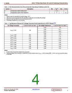
Table 6 shows the minimum current, in addition to I , that is required by Artix-7 devices for proper power-on and
CCQ
configuration. If the current minimums shown in Table 5 and Table 6 are met, the device powers on after all four supplies
have passed through their power-on reset threshold voltages. The FPGA must not be configured until after V is applied.
CCINT
Once initialized and configured, use the Xilinx Power Estimator (XPE) tools to estimate current drain on these supplies.
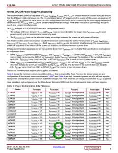
Table 6: Power-On Current for Artix-7 Devices
Device
XC7A12T
ICCINTMIN
ICCAUXMIN
ICCOMIN
ICCBRAMMIN
ICCBRAMQ + 60
ICCBRAMQ + 60
ICCBRAMQ + 60
ICCBRAMQ + 60
ICCBRAMQ + 60
ICCBRAMQ + 60
ICCBRAMQ + 60
ICCBRAMQ + 80
ICCBRAMQ + 60
ICCBRAMQ + 60
ICCBRAMQ + 60
ICCBRAMQ + 60
ICCBRAMQ + 60
ICCBRAMQ + 60
ICCBRAMQ + 60
ICCBRAMQ + 60
Units
mA
mA
mA
mA
mA
mA
mA
mA
mA
mA
mA
mA
mA
mA
mA
mA
ICCINTQ + 120
ICCAUXQ + 40
ICCAUXQ + 40
ICCAUXQ + 40
ICCAUXQ + 40
ICCAUXQ + 40
ICCAUXQ + 40
ICCAUXQ + 40
ICCAUXQ + 50
ICCAUXQ + 40
ICCAUXQ + 40
ICCAUXQ + 40
ICCAUXQ + 40
ICCAUXQ + 40
ICCAUXQ + 40
ICCAUXQ + 40
ICCAUXQ + 40
ICCOQ + 40 mA per bank
ICCOQ + 40 mA per bank
ICCOQ + 40 mA per bank
ICCOQ + 40 mA per bank
ICCOQ + 40 mA per bank
ICCOQ + 40 mA per bank
ICCOQ + 40 mA per bank
ICCOQ + 40 mA per bank
ICCOQ + 40 mA per bank
ICCOQ + 40 mA per bank
ICCOQ + 40 mA per bank
ICCOQ + 40 mA per bank
ICCOQ + 40 mA per bank
ICCOQ + 40 mA per bank
ICCOQ + 40 mA per bank
ICCOQ + 40 mA per bank
XC7A15T
XC7A25T
XC7A35T
XC7A50T
XC7A75T
XC7A100T
XC7A200T
XA7A12T
XA7A15T
XA7A25T
XA7A35T
XA7A50T
XA7A75T
XA7A100T
XQ7A50T
I
CCINTQ + 120
ICCINTQ + 120
CCINTQ + 120
I
ICCINTQ + 120
ICCINTQ + 170
I
CCINTQ + 170
ICCINTQ + 340
ICCINTQ + 120
I
CCINTQ + 120
ICCINTQ + 120
ICCINTQ + 120
ICCINTQ + 120
I
CCINTQ + 170
ICCINTQ + 170
ICCINTQ + 120
DS181 (v1.25) June 18, 2018
www.xilinx.com
Product Specification
8

 XILINX [ XILINX, INC ]