Artix-7 FPGAs Data Sheet: DC and AC Switching Characteristics
(1)(2)
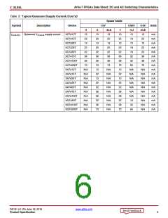
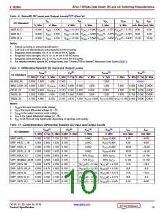
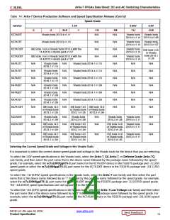
Table 8: SelectIO DC Input and Output Levels
(Cont’d)
VIL
VIH
VOL
VOH
IOL
IOH
I/O Standard
V, Min
–0.300
–0.300
–0.300
V, Max
V, Min
V, Max
V, Max
V, Min
mA, Max mA, Min
SSTL15_R
SSTL18_I
SSTL18_II
VREF – 0.100
VREF + 0.100 VCCO + 0.300 VCCO/2 – 0.175 VCCO/2 + 0.175
VREF + 0.125 VCCO + 0.300 VCCO/2 – 0.470 VCCO/2 + 0.470
8.90
8.00
–8.90
–8.00
V
REF – 0.125
VREF – 0.125
VREF + 0.125 VCCO + 0.300 VCCO/2 – 0.600 VCCO/2 + 0.600 13.40
–13.40
Notes:
1. Tested according to relevant specifications.
2. 3.3V and 2.5V standards are only supported in HR I/O banks.
3. Supported drive strengths of 4, 8, or 12 mA in HR I/O banks.
4. Supported drive strengths of 4, 8, 12, or 16 mA in HR I/O banks.
5. Supported drive strengths of 4, 8, 12, 16, or 24 mA in HR I/O banks.
6. For detailed interface specific DC voltage levels, see 7 Series FPGAs SelectIO Resources User Guide (UG471).
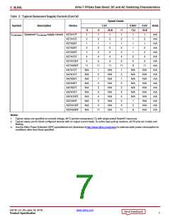
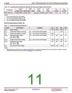
Table 9: Differential SelectIO DC Input and Output Levels
(1)
(2)
(3)
(4)
VICM
V, Min V, Typ V, Max V, Min V, Typ V, Max
0.300 1.200 1.425 0.100
VID
VOCM
VOD
I/O Standard
V, Min
–
V, Typ
1.250
1.200
0.950
1.200
V, Max
–
V, Min V, Typ V, Max
Note 5
BLVDS_25
–
–
MINI_LVDS_25 0.300 1.200 VCCAUX 0.200 0.400 0.600
1.000
0.500
1.000
1.400
1.400
1.400
0.300 0.450 0.600
0.100 0.250 0.400
0.100 0.350 0.600
PPDS_25
RSDS_25
TMDS_33
0.200 0.900 VCCAUX 0.100 0.250 0.400
0.300 0.900
2.700 2.965
1.500
3.230
0.100 0.350 0.600
0.150 0.675 1.200
V
CCO–0.405 VCCO–0.300 VCCO–0.190 0.400 0.600 0.800
Notes:
1.
2.
3.
4.
5.
V
V
V
V
V
is the input common mode voltage.
is the input differential voltage (Q – Q).
ICM
ID
is the output common mode voltage.
OCM
is the output differential voltage (Q – Q).
for BLVDS will vary significantly depending on topology and loading.
OD
OD
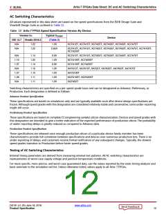
Table 10: Complementary Differential SelectIO DC Input and Output Levels
(1)
(2)
(3)
(4)
VICM
V, Min V,Typ V, Max V,Min V, Max
VID
VOL
VOH
IOL
mA, Max
8.00
IOH
mA, Min
–8.00
–8.00
–16.00
–16.00
–0.100
–0.100
–13.0
–8.9
I/O Standard
V, Max
0.400
V, Min
DIFF_HSTL_I
0.300 0.750 1.125 0.100
0.300 0.900 1.425 0.100
0.300 0.750 1.125 0.100
0.300 0.900 1.425 0.100
0.300 0.600 0.850 0.100
–
–
–
–
–
–
–
–
–
–
–
VCCO–0.400
VCCO–0.400
DIFF_HSTL_I_18
DIFF_HSTL_II
0.400
8.00
0.400
V
CCO–0.400
16.00
16.00
0.100
0.100
13.0
DIFF_HSTL_II_18
DIFF_HSUL_12
0.400
VCCO–0.400
80ꢀ VCCO
90ꢀ VCCO
20ꢀ VCCO
10ꢀ VCCO
DIFF_MOBILE_DDR 0.300 0.900 1.425 0.100
DIFF_SSTL135
DIFF_SSTL135_R
DIFF_SSTL15
0.300 0.675 1.000 0.100
0.300 0.675 1.000 0.100
0.300 0.750 1.125 0.100
0.300 0.750 1.125 0.100
0.300 0.900 1.425 0.100
(VCCO/2) – 0.150 (VCCO/2) + 0.150
(VCCO/2) – 0.150 (VCCO/2) + 0.150
(VCCO/2) – 0.175 (VCCO/2) + 0.175
(VCCO/2) – 0.175 (VCCO/2) + 0.175
(VCCO/2) – 0.470 (VCCO/2) + 0.470
8.9
13.0
–13.0
–8.9
DIFF_SSTL15_R
DIFF_SSTL18_I
8.9
8.00
–8.00
DS181 (v1.25) June 18, 2018
www.xilinx.com
Product Specification
10

 XILINX [ XILINX, INC ]