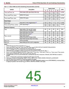
Virtex-6 FPGA Data Sheet: DC and Switching Characteristics
Speed Grade
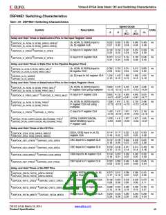
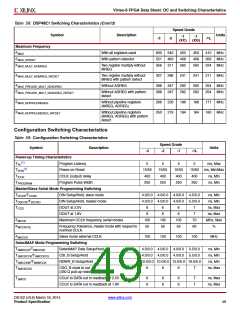
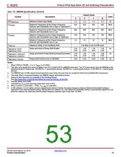
Table 58: DSP48E1 Switching Characteristics (Cont’d)
Symbol
Description
Units
-1
(XC)
-1
(XQ)
-3
-2
-1L
Maximum Frequency
FMAX
With all registers used
With pattern detector
600
551
356
540
483
311
450
408
262
450
408
262
410 MHz
356 MHz
224 MHz
FMAX_PATDET
FMAX_MULT_NOMREG
Two register multiply without
MREG
FMAX_MULT_NOMREG_PATDET
Two register multiply without
MREG with pattern detect
327
286
241
241
211 MHz
FMAX_PREADD_MULT_NOADREG
Without ADREG
398
398
347
347
292
292
292
292
254 MHz
254 MHz
FMAX_PREADD_MULT_NOADREG_PATDET
Without ADREG with pattern
detect
FMAX_NOPIPELINEREG
Without pipeline registers
(MREG, ADREG)
266
250
233
219
196
184
196
184
171 MHz
160 MHz
FMAX_NOPIPELINEREG_PATDET
Without pipeline registers
(MREG, ADREG) with pattern
detect
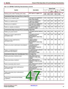
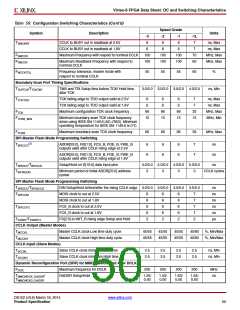
Configuration Switching Characteristics
Table 59: Configuration Switching Characteristics
Speed Grade
Symbol
Description
Units
-3
-2
-1
-1L
Power-up Timing Characteristics
(1)
TPL
Program Latency
Power-on-Reset
5
5
5
5
ms, Max
(1)
TPOR
15/55
400
15/55
400
15/55
400
15/60 ms, Min/Max
TICCK
CCLK (output) delay
Program Pulse Width
400
250
ns, Min
ns, Min
TPROGRAM
250
250
250
Master/Slave Serial Mode Programming Switching
TDCCK/TCCKD
DSCCK/TSCCKD
DIN Setup/Hold, slave mode
DIN Setup/Hold, master mode
DOUT at 2.5V
4.0/0.0 4.0/0.0 4.0/0.0 4.5/0.0
4.0/0.0 4.0/0.0 4.0/0.0 5.0/0.0
ns, Min
ns, Min
ns, Max
ns, Max
MHz, Max
%
T
TCCO
6
6
6
6
6
6
7
7
DOUT at 1.8V
FMCCK
Maximum CCLK frequency, serial modes
105
55
105
55
105
55
70
60
FMCCKTOL
Frequency Tolerance, master mode with respect to
nominal CCLK.
FMSCCK
Slave mode external CCLK
100
100
100
100
MHz
SelectMAP Mode Programming Switching
TSMDCCK/TSMCCKD
SelectMAP Data Setup/Hold
4.0/0.0 4.0/0.0 4.0/0.0 5.5/0.0
4.0/0.0 4.0/0.0 4.0/0.0 5.5/0.0
10.0/0.0 10.0/0.0 10.0/0.0 16.0/0.0
ns, Min
ns, Min
ns, Min
ns, Max
TSMCSCCK/TSMCCKCS
CSI_B Setup/Hold
T
SMCCKW/TSMWCCK
RDWR_B Setup/Hold
TSMCKCSO
CSO_B clock to out
6
6
6
7
(330 Ω pull-up resistor required)
TSMCO
CCLK to DATA out in readback at 2.5V
CCLK to DATA out in readback at 1.8V
6
6
6
6
6
6
7
7
ns, Max
ns, Max
DS152 (v3.6) March 18, 2014
www.xilinx.com
Product Specification
49

 XILINX [ XILINX, INC ]