Virtex-6 FPGA Data Sheet: DC and Switching Characteristics
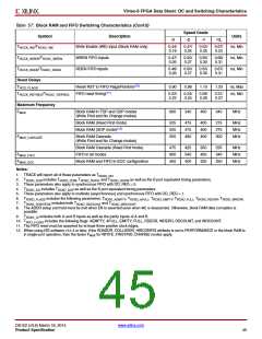
Table 57: Block RAM and FIFO Switching Characteristics (Cont’d)
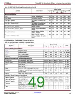
Speed Grade
Symbol
Description
Units
-3
-2
-1
-1L
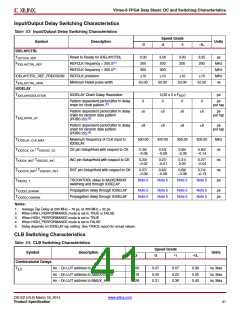
TRCCK_WE/TRCKC_WE
Write Enable (WE) input (Block RAM only)
0.44/
0.19
0.47/
0.25
0.52/
0.35
0.67/
0.24
ns, Min
TRCCK_WREN/TRCKC_WREN
WREN FIFO inputs
RDEN FIFO inputs
0.47/
0.26
0.50/
0.27
0.55/
0.30
0.68/
0.31
ns, Min
ns, Min
T
RCCK_RDEN/TRCKC_RDEN
0.46/
0.26
0.50/
0.27
0.55/
0.30
0.67/
0.31
Reset Delays
TRCO_FLAGS
Reset RST to FIFO Flags/Pointers(10)
FIFO reset timing(11)
0.90
0.98
1.10
1.23
ns, Max
ns, Min
T
RCCK_RSTREG/TRCKC_RSTREG
0.22/
0.23
0.24/
0.24
0.28/
0.26
0.31/
0.27
Maximum Frequency
FMAX
Block RAM in TDP and SDP modes
(Write First and No Change modes)
600
540
450
340
MHz
Block RAM (Read First mode)
Block RAM (SDP mode)(12)
525
525
550
475
475
490
400
400
400
275
275
300
MHz
MHz
MHz
FMAX_CASCADE
Block RAM Cascade
(Write First and No Change modes)
Block RAM Cascade (Read First mode)
FIFO in all modes
475
600
450
425
540
400
350
450
325
235
340
250
MHz
MHz
MHz
FMAX_FIFO
FMAX_ECC
Block RAM and FIFO in ECC configuration
Notes:
1. TRACE will report all of these parameters as T
.
RCKO_DO
2.
3. These parameters also apply to synchronous FIFO with DO_REG = 0.
4. includes T as well as the B port equivalent timing parameters.
5. These parameters also apply to multirate (asynchronous) and synchronous FIFO with DO_REG = 1.
T
includes T
, T
, and T
as well as the B port equivalent timing parameters.
RCKO_DOR
RCKO_DOW RCKO_DOPR
RCKO_DOPW
T
RCKO_DO
RCKO_DOP
6.
7.
T
T
includes the following parameters: T
, T , T , T , T , T
RCKO_FLAGS
RCKO_AEMPTY RCKO_AFULL RCKO_EMPTY RCKO_FULL RCKO_RDERR RCKO_WRERR.
includes both T
and T
RCKO_POINTERS
RCKO_RDCOUNT
RCKO_WRCOUNT.
8. The ADDR setup and hold must be met when EN is asserted (even when WE is deasserted). Otherwise, block RAM data corruption is
possible.
9.
T
includes both A and B inputs as well as the parity inputs of A and B.
RCKO_DI
10. T
includes the following flags: AEMPTY, AFULL, EMPTY, FULL, RDERR, WRERR, RDCOUNT, and WRCOUNT.
RCO_FLAGS
11. The FIFO reset must be asserted for at least three positive clock edges.
12. When using ISE software v12.4 or later, if the RDADDR_COLLISION_HWCONFIG attribute is set to PERFORMANCE or the block RAM is
in single-port operation, then the faster F
for WRITE_FIRST/NO_CHANGE modes apply.
MAX
DS152 (v3.6) March 18, 2014
www.xilinx.com
Product Specification
45

 XILINX [ XILINX, INC ]