Virtex-6 FPGA Data Sheet: DC and Switching Characteristics
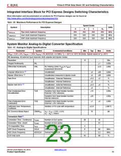
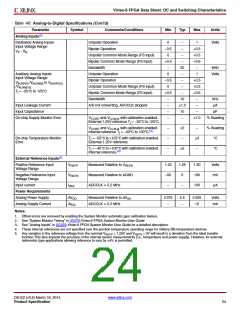
Table 40: Analog-to-Digital Specifications (Cont’d)
Parameter
Analog Inputs(3)
Symbol
Comments/Conditions
Min
Typ
Max
Units
Dedicated Analog Inputs
Input Voltage Range
VP - VN
Unipolar Operation
0
–0.5
0
–
–
1
+0.5
+0.5
+0.6
–
Volts
Bipolar Operation
Unipolar Common Mode Range (FS input)
Bipolar Common Mode Range (FS input)
Bandwidth
–
+0.5
–
–
20
–
MHz
Volts
Auxiliary Analog Inputs
Input Voltage Range
Unipolar Operation
0
1
Bipolar Operation
–0.5
0
–
+0.5
+0.5
+0.6
–
V
AUXP[0] /VAUXN[0] to VAUXP[15]
/VAUXN[15]
Unipolar Common Mode Range (FS input)
Bipolar Common Mode Range (FS input)
Bandwidth
–
Tj = –55°C to 125°C
+0.5
–
–
10
1.0
10
–
kHz
µA
Input Leakage Current
Input Capacitance
A/D not converting, ADCCLK stopped
–
–
–
–
pF
On-chip Supply Monitor Error
V
CCINT and VCCAUX with calibration enabled.
–
1.0
% Reading
External 1.25V reference Tj = –55°C to 125°C.
V
CCINT and VCCAUX with calibration enabled.
–
–
–
2
–
–
4
–
% Reading
Internal reference Tj = –40°C to 100°C.(4)
On-chip Temperature Monitor
Error
Tj = –55°C to +125°C with calibration enabled.
External 1.25V reference.
°C
°C
Tj = –40°C to +100°C with calibration enabled.
Internal reference.(4)
5
External Reference Inputs(5)
Positive Reference Input
Voltage Range
VREFP
VREFN
IREF
Measured Relative to VREFN
Measured Relative to AGND
ADCCLK = 5.2 MHz
1.20
–50
–
1.25
0
1.30
100
100
Volts
mV
µA
Negative Reference Input
Voltage Range
Input current
–
Power Requirements
Analog Power Supply
Analog Supply Current
AVDD
AIDD
Measured Relative to AVSS
ADCCLK = 5.2 MHz
2.375
–
2.5
–
2.625
12
Volts
mA
Notes:
1. Offset errors are removed by enabling the System Monitor automatic gain calibration feature.
2. See "System Monitor Timing" in UG370:Virtex-6 FPGA System Monitor User Guide
3. See "Analog Inputs" in UG370:Virtex-6 FPGA System Monitor User Guide for a detailed description.
4. These internal references are not specified over the junction temperature operating range for military (M) temperature devices.
5. Any variation in the reference voltage from the nominal V = 1.25V and V = 0V will result in a deviation from the ideal transfer
REFP
REFN
function.This also impacts the accuracy of the internal sensor measurements (i.e., temperature and power supply). However, for external
ratiometric type applications allowing reference to vary by 4% is permitted.
DS152 (v3.6) March 18, 2014
www.xilinx.com
Product Specification
24

 XILINX [ XILINX, INC ]