R
XC17V00 Series Configuration PROM
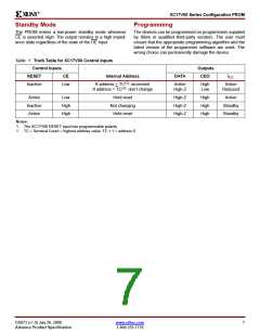
unchanged after configuration is complete. Therefore, to
reprogram the FPGA with another program, the DONE line
is pulled Low and configuration begins at the last value of
the address counters.
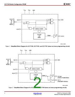
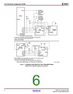
FPGA Master Serial Mode Summary
The I/O and logic functions of the Configurable Logic Block
(CLB) and their associated interconnections are estab-
lished by a configuration program. The program is loaded
either automatically upon power up, or on command,
depending on the state of the three FPGA mode pins. In
Master Serial mode, the FPGA automatically loads the con-
figuration program from an external memory. The Xilinx
PROMs have been designed for compatibility with the Mas-
ter Serial mode.
This method fails if a user applies RESET during the FPGA
configuration process. The FPGA aborts the configuration
and then restarts a new configuration, as intended, but the
PROM does not reset its address counter, since it never
saw a High level on its OE input. The new configuration,
therefore, reads the remaining data in the PROM and inter-
prets it as preamble, length count etc. Since the FPGA is
the master, it issues the necessary number of CCLK pulses,
Upon power-up or reconfiguration, an FPGA enters the
Master Serial mode whenever all three of the FPGA
mode-select pins are Low (M0=0, M1=0, M2=0). Data is
read from the PROM sequentially on a single data line. Syn-
chronization is provided by the rising edge of the temporary
signal CCLK, which is generated during configuration.
24
up to 16 million (2 ) and DONE goes High. However, the
FPGA configuration will be completely wrong, with potential
contentions inside the FPGA and on its output pins. This
method must, therefore, never be used when there is any
chance of external reset during configuration.
Master Serial Mode provides a simple configuration inter-
face. Only a serial data line and two control lines are
required to configure an FPGA. Data from the PROM is
read sequentially, accessed via the internal address and bit
counters which are incremented on every valid rising edge
of CCLK.
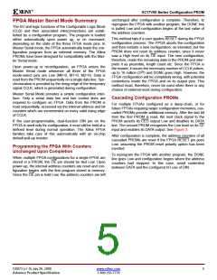
Cascading Configuration PROMs
For multiple FPGAs configured as a daisy-chain, or for
future FPGAs requiring larger configuration memories, cas-
caded PROMs provide additional memory. After the last bit
from the first PROM is read, the next clock signal to the
PROM asserts its CEO output Low and disables its DATA
line. The second PROM recognizes the Low level on its CE
input and enables its DATA output. See Figure 3.
If the user-programmable, dual-function DIN pin on the
FPGA is used only for configuration, it must still be held at a
defined level during normal operation. The Xilinx FPGA
families take care of this automatically with an on-chip
default pull-up resistor.
After configuration is complete, the address counters of all
cascaded PROMs are reset if the FPGA RESET pin goes
Low, assuming the PROM reset polarity option has been
inverted.
Programming the FPGA With Counters
Unchanged Upon Completion
To reprogram the FPGA with another program, the DONE
line goes Low and configuration begins where the address
counters had stopped. In this case, avoid contention
between DATA and the configured I/O use of DIN.
When multiple FPGA-configurations for a single FPGA are
stored in a PROM, the OE pin should be tied Low. Upon
power-up, the internal address counters are reset and con-
figuration begins with the first program stored in memory.
Since the OE pin is held Low, the address counters are left
DS073 (v1.0) July 26, 2000
Advance Product Specification
www.xilinx.com
1-800-255-7778
5

 XILINX [ XILINX, INC ]