R
XC17V00 Series Configuration PROM
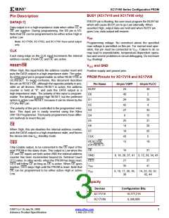
PROM Pinouts for XC17V04, XC17V02, and
XC17V01
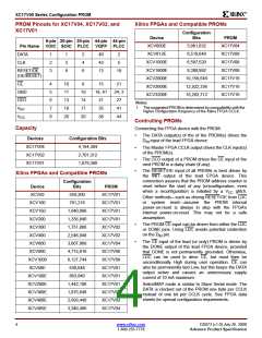
Xilinx FPGAs and Compatible PROMs
Configuration
Device
Bits
PROM
8-pin 20-pin 20-pin 44-pin 44-pin
XCV600E
XCV812E
XCV1000E
XCV1600E
XCV2000E
XCV2600E
XCV3200E
3,961,632
6,519,648
6,587,520
8,308,992
10,159,648
12,922,336
16,283,712
XC17V04
XC17V08
XC17V08
XC17V08
XC17V16
XC17V16
XC17V16
Pin Name VOIC SOIC PLCC VQFP PLCC
DATA
CLK
1
2
3
1
3
8
2
4
6
40
43
13
2
5
RESET/OE
19
(OE/RESET)
CE
4
5
6
7
8
10
11
13
18
20
8
15
18, 41
21
21
24, 3
27
GND
CEO
10
14
17
20
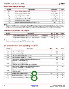
Notes:
1. The suggested PROM is determined by compatibility with the
higher configuration frequency of the Xilinx FPGA CCLK.
V
V
35
41
PP
CC
38
44
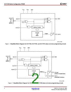
Controlling PROMs
Capacity
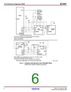
Connecting the FPGA device with the PROM.
•
The DATA output(s) of the of the PROM(s) drives the
input of the lead FPGA device.
Devices
Configuration Bits
4,194,304
D
IN
XC17V04
XC17V02
XC17V01
•
•
•
The Master FPGA CCLK output drives the CLK input(s)
of the PROM(s).
2,701,312
The CEO output of a PROM drives the CE input of the
next PROM in a daisy chain (if any).
1,679,360
The RESET/OE input of all PROMs is best driven by
the INIT output of the lead FPGA device. This
connection assures that the PROM address counter is
reset before the start of any (re)configuration, even
Xilinx FPGAs and Compatible PROMs
Configuration
Device
XCV50
Bits
PROM
when a reconfiguration is initiated by a V
glitch.
CC
559,200
XC17V01
XC17V01
XC17V01
XC17V01
XC17V02
XC17V02
XC17V04
XC17V08
XC17V08
XC17V01
XC17V01
XC17V01
XC17V02
XC17V02
XC17V04
Other methods—such as driving RESET/OE from LDC
or system reset—assume the PROM internal
power-on-reset is always in step with the FPGA’s
internal power-on-reset. This may not be a safe
assumption.
XCV100
XCV150
XCV200
XCV300
XCV400
XCV600
XCV800
XCV1000
XCV50E
XCV100E
XCV200E
XCV300E
XCV400E
XCV405E
781,216
1,040,096
1,335,840
1,751,808
2,546,048
3,607,968
4,715,616
6,127,744
630,048
•
•
The PROM CE input can be driven from either the LDC
or DONE pins. Using LDC avoids potential contention
on the D pin.
IN
The CE input of the lead (or only) PROM is driven by
the DONE output of the lead FPGA device, provided
that DONE is not permanently grounded. Otherwise,
LDC can be used to drive CE, but must then be
unconditionally High during user operation. CE can
also be permanently tied Low, but this keeps the DATA
output active and causes an unnecessary supply
current of 10 mA maximum.
863,840
1,442,106
1,875,648
2,693,440
3,340,400
•
SelectMAP mode is similar to Slave Serial mode. The
DATA is clocked out of the PROM one byte per CCLK
instead of one bit per CCLK cycle. See FPGA data
sheets for special configuration requirements.
4
www.xilinx.com
DS073 (v1.0) July 26, 2000
1-800-255-7778
Advance Product Specification

 XILINX [ XILINX, INC ]