R
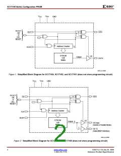
XC17V00 Series Configuration PROM
BUSY (XC17V16 and XC17V08 only)
Pin Description
If BUSY pin is floating, the user must program the BUSY bit
which will cause BUSY pin to go Low internally. When
asserted High, output data are held and when BUSY pin
goes Low, data output will resume.
DATA[0:7]
Data output is in a high-impedance state when either CE or
OE are inactive. During programming, the D0 pin is I/O.
Note that OE can be programmed to be either active High or
active Low.
VPP
Note: XC17V04, XC17V02, and XC17V01 have serial output
only.
Programming voltage. No overshoot above the specified
max voltage is permitted on this pin. For normal read oper-
ation, this pin must be connected to V . Failure to do so
may lead to unpredictable, temperature-dependent opera-
tion and severe problems in circuit debugging. Do not leave
CC
CLK
Each rising edge on the CLK input increments the internal
address counter, if both CE and OE are active.
V
floating!
PP
RESET/OE
VCC and GND
When High, this input holds the address counter reset and
puts the DATA output in a high-impedance state. The polar-
ity of this input pin is programmable as either RESET/OE or
OE/RESET. To avoid confusion, this document describes
the pin as RESET/OE, although the opposite polarity is pos-
sible on all devices. When RESET is active, the address
counter is held at "0", and puts the DATA output in a
high-impedance state. The polarity of this input is program-
mable. The default is active High RESET, but the preferred
option is active Low RESET, because it can be driven by the
FPGAs INIT pin.
Positive supply and ground pins.
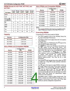
PROM Pinouts for XC17V16 and XC17V08
Pin Name
BUSY
44-pin VQFP
44-pin PLCC
24
40
29
42
27
9
30
2
D0
D1
D2
D3
D4
D5
D6
D7
CLK
35
4
The polarity of this pin is controlled in the programmer inter-
face. This input pin is easily inverted using the Xilinx
HW-130 Programmer. Third-party programmers have differ-
ent methods to invert this pin.
33
15
31
20
25
5
25
14
19
43
13
CE
When High, this pin disables the internal address counter,
puts the DATA output in a high-impedance state, and forces
the device into low-I standby mode.
CC
RESET/OE
19
CEO
(OE/RESET)
Chip Enable output, to be connected to the CE input of the
next PROM in the daisy chain. This output is Low when the
CE and OE inputs are both active AND the internal address
counter has been incremented beyond its Terminal Count
(TC) value. In other words: when the PROM has been read,
CEO will follow CE as long as OE is active. When OE goes
inactive, CEO stays High until the PROM is reset. Note that
OE can be programmed to be either active High or active
Low.
CE
15
21
GND
CEO
6, 18, 28, 27, 41 3, 12, 24, 34, 43
21
35
27
41
V
V
PP
CC
8, 16, 17, 26, 36,
38
14, 22, 23, 32,
42, 44
Capacity
Devices
Configuration Bits
XC17V16
XC17V08
16,777,216
8,388,608
DS073 (v1.0) July 26, 2000
Advance Product Specification
www.xilinx.com
1-800-255-7778
3

 XILINX [ XILINX, INC ]