R
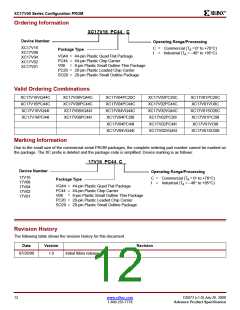
XC17V00 Series Configuration PROM
Absolute Maximum Ratings
Symbol
Description
Conditions
–0.5 to +7.0
–0.5 to +12.5
Units
V
V
Supply voltage relative to GND
CC
PP
V
Supply voltage relative to GND
V
V
Input voltage relative to GND
–0.5 to V +0.5
V
IN
CC
V
Voltage applied to High-Z output
Storage temperature (ambient)
–0.5 to V +0.5
V
TS
CC
T
–65 to +150
°C
°C
STG
SOL
T
Maximum soldering temperature (10s @ 1/16 in.)
+260
Notes:
1. Stresses beyond those listed under Absolute Maximum Ratings may cause permanent damage to the device. These are stress
ratings only, and functional operation of the device at these or any other conditions beyond those listed under Operating Conditions
is not implied. Exposure to Absolute Maximum Ratings conditions for extended periods of time may affect device reliability.
Operating Conditions (3V Supply)
Symbol
Description
Supply voltage relative to GND (T = 0°C to +70°C)
Min
3.0
3.0
Max
3.6
Units
(1)
V
Commercial
Industrial
V
V
CC
A
Supply voltage relative to GND (T = –40°C to +85°C)
3.6
A
Notes:
1. During normal read operation VPP MUST be connect to V
CC.
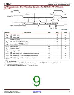
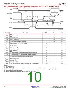
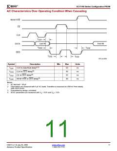
DC Characteristics Over Operating Condition
Symbol
Description
Min
Max
Units
V
V
High-level input voltage
Low-level input voltage
2
0
V
CC
IH
V
0.8
-
V
IL
V
High-level output voltage (I = –3 mA)
2.4
-
V
OH
OH
V
Low-level output voltage (I = +3 mA)
0.4
100
V
OL
OL
I
I
I
I
Supply current, standby mode (at maximum frequency)
(XC17V16 and XC17V08 only)
-
mA
CCA
CCS
CCA
CCS
Supply current, standby mode
(XC17V16, XC17V08, XC17V04, XC17V02 only)
-
-
-
350
10
µA
mA
µA
Supply current, standby mode (at maximum frequency)
(XC17V04, XC17V02, and XC17V01 only)
Supply current, standby mode
50
(XC17V01 only)
I
Input or output leakage current
–10
10
10
10
µA
pF
pF
L
C
Input capacitance (V = GND, f = 1.0 MHz)
-
-
IN
IN
C
Output capacitance (V = GND, f = 1.0 MHz)
IN
OUT
8
www.xilinx.com
1-800-255-7778
DS073 (v1.0) July 26, 2000
Advance Product Specification

 XILINX [ XILINX, INC ]