R
XC17V00 Series Configuration PROM
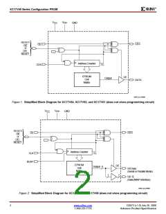
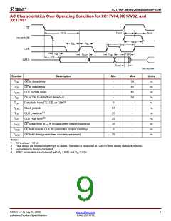
V
V
PP
GND
CC
RESET/
CEO
CE
OE
or
OE/
RESET
Address Counter
CLK
TC
EPROM
Cell
Matrix
OE
Output
DATA
DS073_01_072600
Figure 1: Simplified Block Diagram for XC17V04, XC17V02, and XC17V01 (does not show programming circuit)
V
V
PP
GND
CC
RESET/
OE
or
CEO
CE
OE/
RESET
Address Counter
CLK
TC
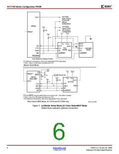
BUSY
EPROM
Cell
Matrix
OE
7
8
Output
D0 Data
(Serial or Parallel Mode)
7
D[1:7]
(SelectMAP Interface)
DS073_02_072600
Figure 2: Simplified Block Diagram for XC17V16 and XC17V08 (does not show programming circuit)
2
www.xilinx.com
DS073 (v1.0) July 26, 2000
1-800-255-7778
Advance Product Specification

 XILINX [ XILINX, INC ]