Spartan-6 FPGA Data Sheet: DC and Switching Characteristics
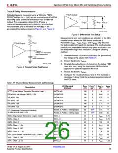
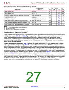
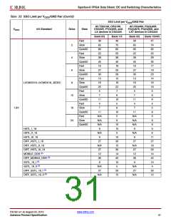
Table 31: Output Delay Measurement Methodology (Cont’d)
(1)
I/O Standard
Attribute
R
C
V
V
REF
REF
REF
MEAS
Description
(Ω)
(pF)
(V)
(V)
1.25
0.75
1.2
0
SSTL, Class II, 2.5V
SSTL, Class II, 1.5V
SSTL2_II
25
0
0
0
0
0
0
0
0
VREF
VREF
0(3)
SSTL15_II
25
LVDS (Low-Voltage Differential Signaling), 2.5V & 3.3V
BLVDS (Bus LVDS), 2.5V
LVDS_25, LVDS_33
BLVDS_25
100
100
100
100
100
100
0(3)
Mini-LVDS, 2.5V & 3.3V
MINI_LVDS_25, MINI_LVDS_33
0(3)
1.2
1.2
RSDS (Reduced Swing Differential Signaling), 2.5V & 3.3V RSDS_25, RSDS_33
0(3)
TMDS (Transition Minimized Differential Signaling), 3.3V
PPDS (Point-to-Point Differential Signaling, 2.5V & 3.3V
TMDS_33
0(3)
PPDS_25, PPDS_33
0(3)
–
Notes:
1.
C
is the capacitance of the probe, nominally 0 pF.
REF
2. Per PCI specifications.
3. The value given is the differential output voltage.
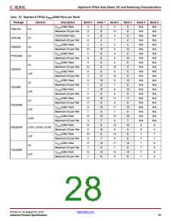
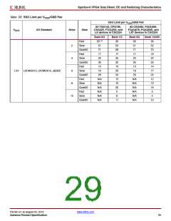
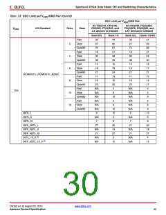
Simultaneously Switching Outputs
Due to lead inductance, a given package supports a limited number of simultaneous switching outputs (SSOs) when using
fast, high-drive outputs. Table 32 and Table 33 provide guidelines for the recommended maximum allowable number of
SSOs. These guidelines describe the maximum number of user I/O pins of an output signal standard that should
simultaneously switch in the same direction, while maintaining a safe level of switching noise for that particular signal
standard. Meeting these guidelines for the stated test conditions ensures that the FPGA operates free from the adverse
effects of GND and power bounce.
For each device/package combination, Table 32 provides the number of equivalent VCCO/GND pairs per bank. For each
output signal standard and drive strength, Table 33 recommends the maximum number of SSOs, switching in the same
direction, allowed per VCCO/GND pair within an I/O bank. The guidelines are categorized by package style, slew rate, and
output drive current. The number of SSOs are also specified by I/O bank. Multiply the appropriate numbers from each table
to calculate the maximum number of SSOs allowed within an I/O bank. The guidelines assume that all pins within a bank use
the same I/O standard. Exceeding these SSO guidelines can result in increased power or GND bounce, degraded signal
integrity, or increased system jitter. For a given I/O standard, if the SSO limit per pair in Table 33 is greater than the maximum
I/O per pair in Table 32, then there is no SSO limit for the exclusive use of that I/O standard.
The recommended maximum SSO values assume that the FPGA is soldered on a printed circuit board and that the board
uses sound design practices. Due to the additional lead inductance introduced by the socket, the SSO values do not apply
for FPGAs mounted in sockets. The SSO values assume that the VCCAUX is powered at 3.3V. Setting VCCAUX to 2.5V
provides better SSO characteristics. For more detail, see the Spartan-6 FPGA SelectIO Resources User Guide.
DS162 (v1.9) August 23, 2010
www.xilinx.com
Advance Product Specification
27

 XILINX [ XILINX, INC ]