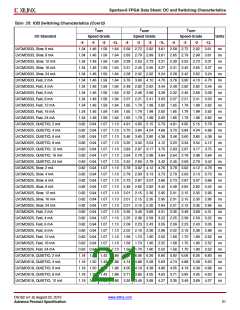
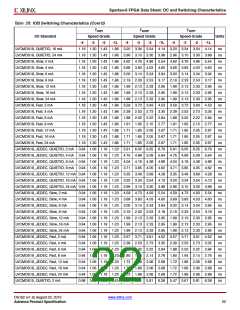
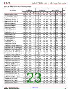
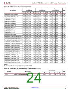
Spartan-6 FPGA Data Sheet: DC and Switching Characteristics
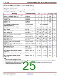
I/O Standard Adjustment Measurement Methodology
Input Delay Measurements
Table 30 shows the test setup parameters used for measuring input delay.
Table 30: Input Delay Measurement Methodology
(1)
(1)
(3)(4)
(2)(4)
Description
LVTTL (Low-Voltage Transistor-Transistor Logic)
LVCMOS (Low-Voltage CMOS), 3.3V
LVCMOS, 2.5V
I/O Standard Attribute
LVTTL
V
V
V
V
L
H
MEAS
REF
0
0
0
0
0
0
3.0
3.3
2.5
1.8
1.5
1.2
1.4
–
LVCMOS33
1.65
1.25
0.9
–
–
–
–
–
–
LVCMOS25
LVCMOS, 1.8V
LVCMOS18
LVCMOS, 1.5V
LVCMOS15
0.75
0.6
LVCMOS, 1.2V
LVCMOS12
PCI (Peripheral Component Interface),
33 MHz and 66 MHz, 3.3V
PCI33_3, PCI66_3
Per PCI Specification
HSTL (High-Speed Transceiver Logic),
Class I & II
HSTL_I, HSTL_II
VREF – 0.5
VREF + 0.5
VREF
0.75
HSTL, Class III
HSTL_III
V
V
V
REF – 0.5
REF – 0.5
REF – 0.5
VREF + 0.5
VREF + 0.5
VREF + 0.5
VREF
VREF
VREF
VREF
0.90
0.90
1.1
HSTL, Class I & II, 1.8V
HSTL, Class III 1.8V
HSTL_I_18, HSTL_II_18
HSTL_III_18
SSTL (Stub Terminated Transceiver Logic),
Class I & II, 3.3V
SSTL3_I, SSTL3_II
VREF – 0.75 VREF + 0.75
1.5
SSTL, Class I & II, 2.5V
SSTL, Class I & II, 1.8V
SSTL, Class II, 1.5V
SSTL2_I, SSTL2_II
SSTL18_I, SSTL18_II
SSTL15_II
VREF – 0.75 VREF + 0.75
VREF
VREF
VREF
0(5)
1.25
0.90
0.75
–
VREF – 0.5
REF – 0.2
VREF + 0.5
VREF + 0.2
V
LVDS (Low-Voltage Differential Signaling),
2.5V & 3.3V
LVDS_25, LVDS_33
1.25 – 0.125 1.25 + 0.125
LVPECL (Low-Voltage Positive Emitter-Coupled
Logic), 2.5V & 3.3V
LVPECL_25, LVPECL_33
1.2 – 0.3
1.2 – 0.3
0(5)
–
BLVDS (Bus LVDS), 2.5V
Mini-LVDS, 2.5V & 3.3V
BLVDS_25
1.3 – 0.125
1.2 – 0.125
1.3 + 0.125
1.2 + 0.125
0(5)
0(5)
–
–
MINI_LVDS_25,
MINI_LVDS_33
RSDS (Reduced Swing Differential Signaling),
2.5V & 3.3V
RSDS_25, RSDS_33
1.2 – 0.1
3.0 – 0.1
1.25 – 0.1
1.2 + 0.1
3.0 + 0.1
1.25 + 0.1
0(5)
0(5)
0(5)
–
–
–
TMDS (Transition Minimized Differential Signaling),
3.3V
TMDS_33
PPDS (Point-to-Point Differential Signaling,
2.5V & 3.3V
PPDS_25, PPDS_33
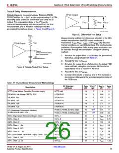
Notes:
1. Input waveform switches between V and V .
L
H
2. Measurements are made at typical, minimum, and maximum V
values. Reported delays reflect worst case of these measurements. V
values
REF
REF
listed are typical.
3. Input voltage level from which measurement starts.
4. This is an input voltage reference that bears no relation to the V
5. The value given is the differential input voltage.
/ V
parameters found in IBIS models and/or noted in Figure 4.
REF
MEAS
DS162 (v1.9) August 23, 2010
www.xilinx.com
Advance Product Specification
25

 XILINX [ XILINX, INC ]