Spartan-6 FPGA Data Sheet: DC and Switching Characteristics
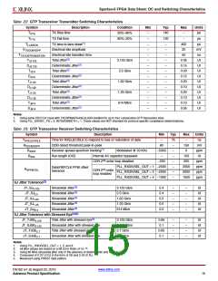
Table 20: GTP Transceiver Reference Clock Switching Characteristics
All LXT Speed Grades
Symbol
Description
Conditions
Units
Min
Typ
–
Max
FGCLK
TRCLK
TFCLK
Reference clock frequency range
Reference clock rise time
Reference clock fall time
60
–
160
–
MHz
ps
20% – 80%
80% – 20%
200
200
50
–
–
ps
TDCREF Reference clock duty cycle
Transceiver PLL only
45
–
55
1
%
TLOCK Clock recovery frequency acquisition Initial PLL lock
–
ms
time
TPHASE Clock recovery phase acquisition time Lock to data after PLL has locked to
the reference clock
–
–
200
µs
X-Ref Target - Figure 3
TRCLK
80%
20%
TFCLK
ds162_05_042109
Figure 3: Reference Clock Timing Parameters
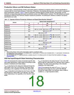
Table 21: GTP Transceiver User Clock Switching Characteristics(1)
Speed Grade
Symbol
Description
Conditions
Units
-4
320
-3
320
-2
-1L
FTXOUT
FRXREC
TRX
TXOUTCLK maximum frequency
RXRECCLK maximum frequency
RXUSRCLK maximum frequency
RXUSRCLK2 maximum frequency
270
270
270
125
125
67.5
270
125
125
67.5
N/A
N/A
N/A
N/A
N/A
N/A
N/A
N/A
N/A
N/A
MHz
MHz
MHz
MHz
MHz
MHz
MHz
MHz
MHz
MHz
320
320
320
320
TRX2
1 byte interface
2 byte interface
4 byte interface
156.25
160
156.25
160
80
80
TTX
TXUSRCLK maximum frequency
TXUSRCLK2 maximum frequency
320
320
TTX2
1 byte interface
2 byte interface
4 byte interface
156.25
160
156.25
160
80
80
Notes:
1. Clocking must be implemented as described in the Spartan-6 FPGA GTP Transceivers User Guide.
DS162 (v1.9) August 23, 2010
www.xilinx.com
Advance Product Specification
14

 XILINX [ XILINX, INC ]