Spartan-6 FPGA Data Sheet: DC and Switching Characteristics
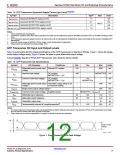
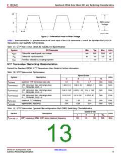
X-Ref Target - Figure 2
+V
0
Differential
Voltage
P–N
–V
ds162_02_112009
Figure 2: Differential Peak-to-Peak Voltage
Table 17 summarizes the DC specifications of the clock input of the GTP transceiver. Consult the Spartan-6 FPGA GTP
Transceivers User Guide for further details.
Table 17: GTP Transceiver Clock DC Input Level Specification
Symbol
VIDIFF
RIN
DC Parameter
Differential peak-to-peak input voltage
Min
200
80
Typ
800
100
100
Max
2000
120
–
Units
mV
Ω
Differential input resistance
CEXT
Required external AC coupling capacitor
–
nF
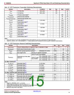
GTP Transceiver Switching Characteristics
Consult the Spartan-6 FPGA GTP Transceivers User Guide for further information.
Table 18: GTP Transceiver Performance
Speed Grade
Symbol
Description
Units
-4
3.2
-3
-2
-1L
FGTPMAX
Maximum GTP transceiver data rate
3.2
2.7
N/A
N/A
Gb/s
Gb/s
FGTPRANGE1
FGTPRANGE2
FGTPRANGE3
GTP transceiver data rate range when
PLL_TXDIVSEL_OUT = 1
1.88 to 3.2
1.88 to 3.2
1.88 to 2.7
GTP transceiver data rate range when
PLL_TXDIVSEL_OUT = 2
0.94 to 1.62 0.94 to 1.62 0.94 to 1.62
N/A
N/A
Gb/s
Gb/s
GTP transceiver data rate range when
PLL_TXDIVSEL_OUT = 4
0.6 to 0.81
0.6 to 0.81
0.6 to 0.81
FGPLLMAX
FGPLLMIN
Maximum PLL frequency
Minimum PLL frequency
1.62
0.94
1.62
0.94
1.62
0.94
N/A
N/A
GHz
GHz
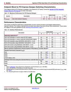
Table 19: GTP Transceiver Dynamic Reconfiguration Port (DRP) Switching Characteristics
Speed Grade
Symbol
Description
Units
-4
-3
-2
-1L
N/A
FGTPDRPCLK
GTP transceiver DCLK (DRP clock) maximum frequency
160
125
100
MHz
DS162 (v1.9) August 23, 2010
www.xilinx.com
Advance Product Specification
13

 XILINX [ XILINX, INC ]