Spartan-6 FPGA Data Sheet: DC and Switching Characteristics
GTP Transceiver Specifications
GTP transceivers are available in the Spartan-6 LXT family of devices. See DS160: Spartan-6 Family Overview for more
information.
GTP Transceiver DC Characteristics
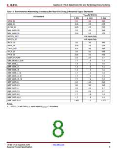
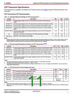
Table 12: Absolute Maximum Ratings for GTP Transceivers(1)
Symbol
Description
MIn
Max
Units
MGTAVCC
Analog supply voltage for the GTP transmitter and receiver circuits relative to
GND
–0.5
1.32
V
MGTAVTTTX
MGTAVTTRX
MGTAVCCPLL
Analog supply voltage for the GTP transmitter termination circuit relative to GND
Analog supply voltage for the GTP receiver termination circuit relative to GND
–0.5
–0.5
–0.5
1.32
1.32
1.32
V
V
V
Analog supply voltage for the GTP transmitter and receiver PLL circuits relative to
GND
MGTAVTTRCAL Analog supply voltage for the resistor calibration circuit of the GTP transceiver
bank (top or bottom)
–0.5
1.32
V
VIN
Receiver (RXP/RXN) and Transmitter (TXP/TXN) absolute input voltage
Reference clock absolute input voltage
–0.5
–0.5
1.32
1.32
V
V
VMGTREFCLK
Notes:
1. Stresses beyond those listed under Absolute Maximum Ratings might cause permanent damage to the device. These are stress ratings only, and
functional operation of the device at these or any other conditions beyond those listed under Operating Conditions is not implied. Exposure to
Absolute Maximum Ratings conditions for extended periods of time might affect device reliability.
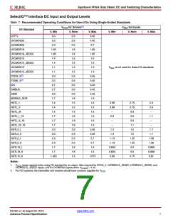
Table 13: Recommended Operating Conditions for GTP Transceivers(1)(2)(3)
Symbol
Description
Min
Typ
1.20
1.20
1.20
1.20
Max
1.26
1.26
1.26
1.26
Units
MGTAVCC
Analog supply voltage for the GTP transmitter and receiver circuits relative to GND 1.14
Analog supply voltage for the GTP transmitter termination circuit relative to GND 1.14
V
V
V
V
MGTAVTTTX
MGTAVTTRX
Analog supply voltage for the GTP receiver termination circuit relative to GND
1.14
MGTAVCCPLL Analog supply voltage for the GTP transmitter and receiver PLL circuits relative to 1.14
GND
MGTAVTTRCAL Analog supply voltage for the resistor calibration circuit of the GTP transceiver
bank (top or bottom)
1.14
1.20
1.26
V
Notes:
1. Each voltage listed requires the filter circuit described in Spartan-6 FPGA GTP Transceivers User Guide.
2. Voltages are specified for the temperature range of T = –40°C to +100°C.
j
3. The voltage level of MGTAVCCPLL must not exceed the voltage level of MGTAVCC +10mV. The voltage level of MGTAVCC must not exceed the
voltage level of MGTAVCCPLL.
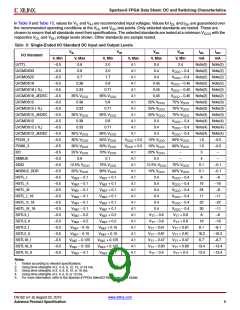
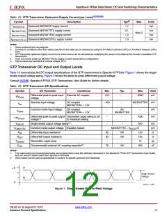
Table 14: GTP Transceiver Current Supply (per Lane)
(1)
Symbol
IMGTAVCC
Description
GTP transceiver internal analog supply current
GTP transmitter termination supply current
Typ
40.4
27.4
13.6
28.7
Max
Units
mA
mA
mA
mA
Ω
IMGTAVTTTX
IMGTAVTTRX
IMGTAVCCPLL
RMGTRREF
Note 2
GTP receiver termination supply current
GTP transmitter and receiver PLL supply current
Precision reference resistor for internal calibration termination
50.0 1%
tolerance
Notes:
1. Typical values are specified at nominal voltage, 25°C, with a 2.5 Gb/s line rate, with a shared PLL use mode.
2. Values for currents of other transceiver configurations and conditions can be obtained by using the XPOWER Estimator (XPE) or XPOWER Analyzer
(XPA) tools.
DS162 (v1.9) August 23, 2010
www.xilinx.com
Advance Product Specification
11

 XILINX [ XILINX, INC ]