R
Platform Flash In-System Programmable Configuration PROMs
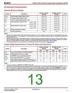
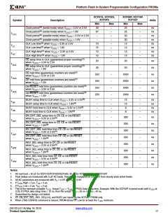
DC Electrical Characteristics
Absolute Maximum Ratings
XCF01S, XCF02S,
XCF04S
XCF08P, XCF16P,
XCF32P
Symbol
Description
Units
VCCINT
VCCO
VCCJ
VIN
Internal supply voltage relative to GND
I/O supply voltage relative to GND
JTAG I/O supply voltage relative to GND
Input voltage with respect to GND
–0.5 to +4.0
–0.5 to +4.0
–0.5 to +4.0
–0.5 to +3.6
–0.5 to +5.5
–0.5 to +3.6
–0.5 to +5.5
–65 to +150
+125
–0.5 to +2.7
–0.5 to +4.0
–0.5 to +4.0
–0.5 to +3.6
–0.5 to +3.6
–0.5 to +3.6
–0.5 to +3.6
–65 to +150
+125
V
V
V
VCCO < 2.5V
VCCO ≥ 2.5V
VCCO < 2.5V
VCCO ≥ 2.5V
V
V
VTS
Voltage applied to High-Z output
V
V
TSTG
TJ
Storage temperature (ambient)
Junction temperature
°C
°C
Notes:
1. Maximum DC undershoot below GND must be limited to either 0.5V or 10 mA, whichever is easier to achieve. During transitions, the device
pins can undershoot to –2.0V or overshoot to +7.0V, provided this overshoot or undershoot lasts less then 10 ns and with the forcing current
being limited to 200 mA.
2. Stresses beyond those listed under Absolute Maximum Ratings might cause permanent damage to the device. These are stress ratings
only, and functional operation of the device at these or any other conditions beyond those listed under Operating Conditions is not implied.
Exposure to Absolute Maximum Ratings conditions for extended periods of time adversely affects device reliability.
3. For soldering guidelines, see the information on "Packaging and Thermal Characteristics" at www.xilinx.com.
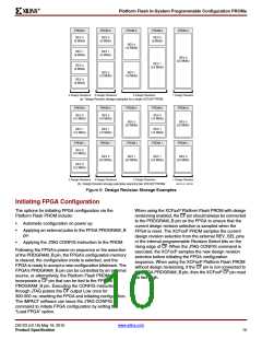
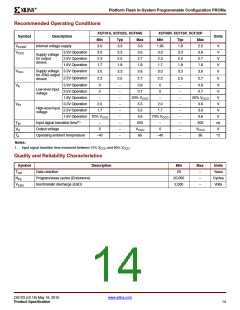
Supply Voltage Requirements for Power-On Reset and Power-Down
XCF01S, XCF02S,
XCF04S
XCF08P, XCF16P,
XCF32P
Symbol
Description
Units
Min
0.2
1
Max
50
–
Min
0.2
0.5
0.5
–
Max
50
TVCC
VCCPOR
TOER
VCCPD
TRST
VCCINT rise time from 0V to nominal voltage(2)
POR threshold for the VCCINT supply
ms
V
–
OE/RESET release delay following POR(3)
0.5
–
3
30
ms
V
Power-down threshold for VCCINT supply
1
0.5
Time required to trigger a device reset when the VCCINT
supply drops below the maximum VCCPD threshold
10
–
10
–
ms
Notes:
1.
V
, V
, and V
supplies can be applied in any order.
CCINT CCO
CCJ
2. At power up, the device requires the V
power supply to monotonically rise to the nominal operating voltage within the specified T
rise
CCINT
VCC
time. If the power supply cannot meet this requirement, then the device might not perform power-on-reset properly. See Figure 6, page 11.
3. If the V and V supplies do not reach their respective recommended operating conditions before the OE/RESET pin is released,
CCINT
CCO
then the configuration data from the PROM is not available at the recommended threshold levels. The configuration sequence must be
delayed until both V and V have reached their recommended operating conditions.
CCINT
CCO
DS123 (v2.18) May 19, 2010
www.xilinx.com
Product Specification
13

 XILINX [ XILINX, INC ]