R
Platform Flash In-System Programmable Configuration PROMs
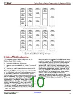
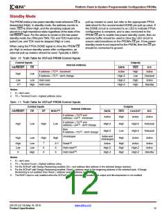
Reset and Power-On Reset Activation
At power up, the device requires the V
power supply to
below the power-down threshold (V
), the PROM resets
CCINT
CCPD
monotonically rise to the nominal operating voltage within
the specified V rise time. If the power supply cannot
meet this requirement, then the device might not perform
power-on reset properly. During the power-up sequence,
OE/RESET is held Low by the PROM. Once the required
supplies have reached their respective POR (Power On
and OE/RESET is again held Low until the after the POR
threshold is reached. OE/RESET polarity is not
programmable. These power-up requirements are shown
graphically in Figure 6.
CCINT
For a fully powered Platform Flash PROM, a reset occurs
whenever OE/RESET is asserted (Low) or CE is deasserted
(High). The address counter is reset, CEO is driven High, and
the remaining outputs are placed in a high-impedance state.
Reset) thresholds, the OE/RESET release is delayed (T
OER
minimum) to allow more margin for the power supplies to
stabilize before initiating configuration. The OE/RESET pin
is connected to an external 4.7 kΩ pull-up resistor and also
to the target FPGA's INIT pin. For systems utilizing slow-
rising power supplies, an additional power monitoring circuit
can be used to delay the target configuration until the
system power reaches minimum operating voltages by
holding the OE/RESET pin Low. When OE/RESET is
released, the FPGA’s INIT pin is pulled High allowing the
FPGA's configuration sequence to begin. If the power drops
Note:
1. The XCFxxS PROM only requires V
to rise above
CCINT
its POR threshold before releasing OE/RESET.
2. The XCFxxP PROM requires both V to rise above its
CCINT
POR threshold and for V
to reach the recommended
CCO
operating voltage level before releasing OE/RESET.
X-Ref Target - Figure 6
VCCINT
Recommended Operating Range
Delay or Restart
Configuration
50 ms ramp
200 µs ramp
VCCPOR
VCCPD
A slow-ramping V
supply may still
CCINT
be below the minimum operating
voltage when OE/RESET is released.
In this case, the configuration
sequence must be delayed until both
V
and V
have reached their
CCINT
CCO
TIME (ms)
recommended operating conditions.
TOER
TOER
TRST
ds123_21_103103
Figure 6: Platform Flash PROM Power-Up Requirements
I/O Input Voltage Tolerance and Power Sequencing
The I/Os on each re-programmable Platform Flash PROM
are fully 3.3V-tolerant. This allows 3V CMOS signals to
connect directly to the inputs without damage. The core
power supply (V
), JTAG pin power supply (V
),
CCINT
CCJ
output power supply (V
), and external 3V CMOS I/O
CCO
signals can be applied in any order.
Additionally, for the XCFxxS PROM only, when V
is
CCO
supplied at 2.5V or 3.3V and V
is supplied at 3.3V, the
CCINT
I/Os are 5V-tolerant. This allows 5V CMOS signals to
connect directly to the inputs on a powered XCFxxS PROM
without damage. Failure to power the PROM correctly while
supplying a 5V input signal can result in damage to the
XCFxxS device.
DS123 (v2.18) May 19, 2010
www.xilinx.com
Product Specification
11

 XILINX [ XILINX, INC ]